Microwave transistor of patterned grid structure and manufacturing method thereof

A patterning and transistor technology, which is applied in semiconductor/solid-state device manufacturing, electrical solid-state devices, semiconductor devices, etc., can solve problems affecting the quality of epitaxial materials, avoid the decline of two-dimensional electron gas density, and make the process simple and routine. Effect

Active Publication Date: 2016-10-12
XIAMEN SANAN INTEGRATED CIRCUIT
View PDF4 Cites 3 Cited by
  • Summary
  • Abstract
  • Description
  • Claims
  • Application Information

AI Technical Summary

Problems solved by technology

However, this puts forward very high requirements on the epitaxial process, because different semiconductor crystal materials have different growth temperatures, and frequent switching of temperatures will affect the final quality of epitaxial materials
None of the above methods can better solve the existing problems

Method used


Image

  • Microwave transistor of patterned grid structure and manufacturing method thereof
  • Microwave transistor of patterned grid structure and manufacturing method thereof
  • Microwave transistor of patterned grid structure and manufacturing method thereof

Examples


Embodiment Construction

[0030] The present invention will be described in further detail below in conjunction with the accompanying drawings and embodiments. The drawings of the present invention are only schematic diagrams for easier understanding of the present invention, and their specific proportions can be adjusted according to design requirements. Those skilled in the art should understand that the upper and lower relationships of relative components in the figures described herein refer to the relative positions of the components, so all of them can be turned over to present the same components, which should all fall within the scope of the present specification. In addition, the numbers of components and structures shown in the figure are only examples, and are not intended to limit the numbers, and can be adjusted according to actual design requirements.

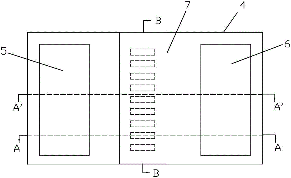
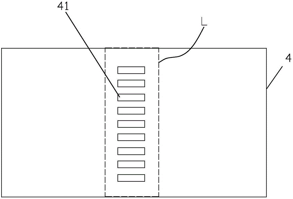
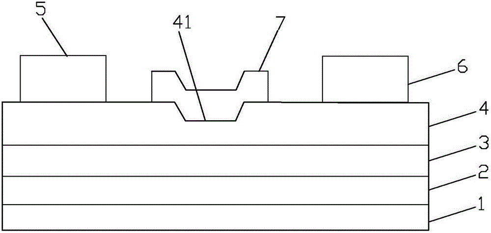
[0031] refer to Figure 1 to Figure 5 , a microwave transistor with a patterned gate structure includes a substrate 1, a buffer layer 2,...


PUM


Abstract

The invention discloses a microwave transistor of a patterned grid structure. The transistor is provided with a patterned region between the source electrode and the drain electrode of a barrier layer. Within the patterned region, the surface of the barrier layer partially concaves downwards along the thickness direction to form a plurality of grooves. A grid is arranged to cover the patterned region. The length of the grid is larger than the lengths of the grooves along the length direction of the grid, so that the grid can completely cover the grooves. On one hand, by means of the grooves, the grid control capability of a device is improved and the short-channel effect is suppressed. On the other hand, an original heterostructure below the grid is preserved. In this way, the reduction of the conductive capacity due to the density reduction of two-dimensional electron gas can be avoided. Therefore, the current output capability of the device is ensured while the short-channel effect is suppressed at the same time. The invention also discloses a manufacturing method of the above microwave transistor.

Description

technical field [0001] The invention relates to a semiconductor device, in particular to a microwave transistor with a patterned gate structure and a preparation method thereof. Background technique [0002] A high electron mobility transistor (HEMT) includes a substrate, a buffer layer, a channel layer, a barrier layer, and a source, drain, and gate on the barrier layer. The two-dimensional electron gas layer (2-2DEG) that exists at the heterojunction interface between the source and the drain controls the electron concentration of the 2-DEG by changing the gate voltage between the source and the drain, thereby controlling the working state. HEMTs are a new generation of transistors that are the first choice for high-frequency, high-voltage, high-temperature and high-power applications due to their excellent performance. [0003] At present, based on the common HEMT structure, the improvement of the frequency performance of microwave devices mainly depends on reducing the ...

Claims


Application Information

Patent Timeline
Patent Type & Authority Applications(China)
IPC IPC(8): H01L29/778H01L29/06H01L21/335H01L29/423H01L21/28
CPCH01L21/28H01L29/06H01L29/42316H01L29/66431H01L29/778H01L21/28587H01L29/2003H01L29/475H01L29/7786H01L21/28581H01L21/32133H01L23/66H01L29/205H01L29/66462H01L2223/6683
Inventor 刘胜厚叶念慈黄侯魁
Owner XIAMEN SANAN INTEGRATED CIRCUIT
Why Eureka
Try Eureka