Carrier storage type igbt and manufacturing method thereof

A technology of carrier storage and manufacturing method, which is applied in the manufacture of carrier storage IGBTs and the field of carrier storage IGBTs, can solve the problems of increasing the on-voltage drop of the device and reducing the anti-latch capability of the device, etc. Achieve enhanced memory effect, improved turn-on voltage drop and latch-up resistance

Active Publication Date: 2019-06-11
SHANGHAI HUAHONG GRACE SEMICON MFG CORP
View PDF4 Cites 0 Cited by
  • Summary
  • Abstract
  • Description
  • Claims
  • Application Information

AI Technical Summary

Problems solved by technology

However, under the action of the electric field, part of the holes injected on the back side will be swept out of the drift region by the electric field, as shown by the arrow line 121, and flow out through the contact hole, which is the so-called hole current; the hole current will increase the conduction of the device voltage drop and degrades the device's immunity to latch-up

Method used


Image

  • Carrier storage type igbt and manufacturing method thereof
  • Carrier storage type igbt and manufacturing method thereof
  • Carrier storage type igbt and manufacturing method thereof

Examples


no. 1 example

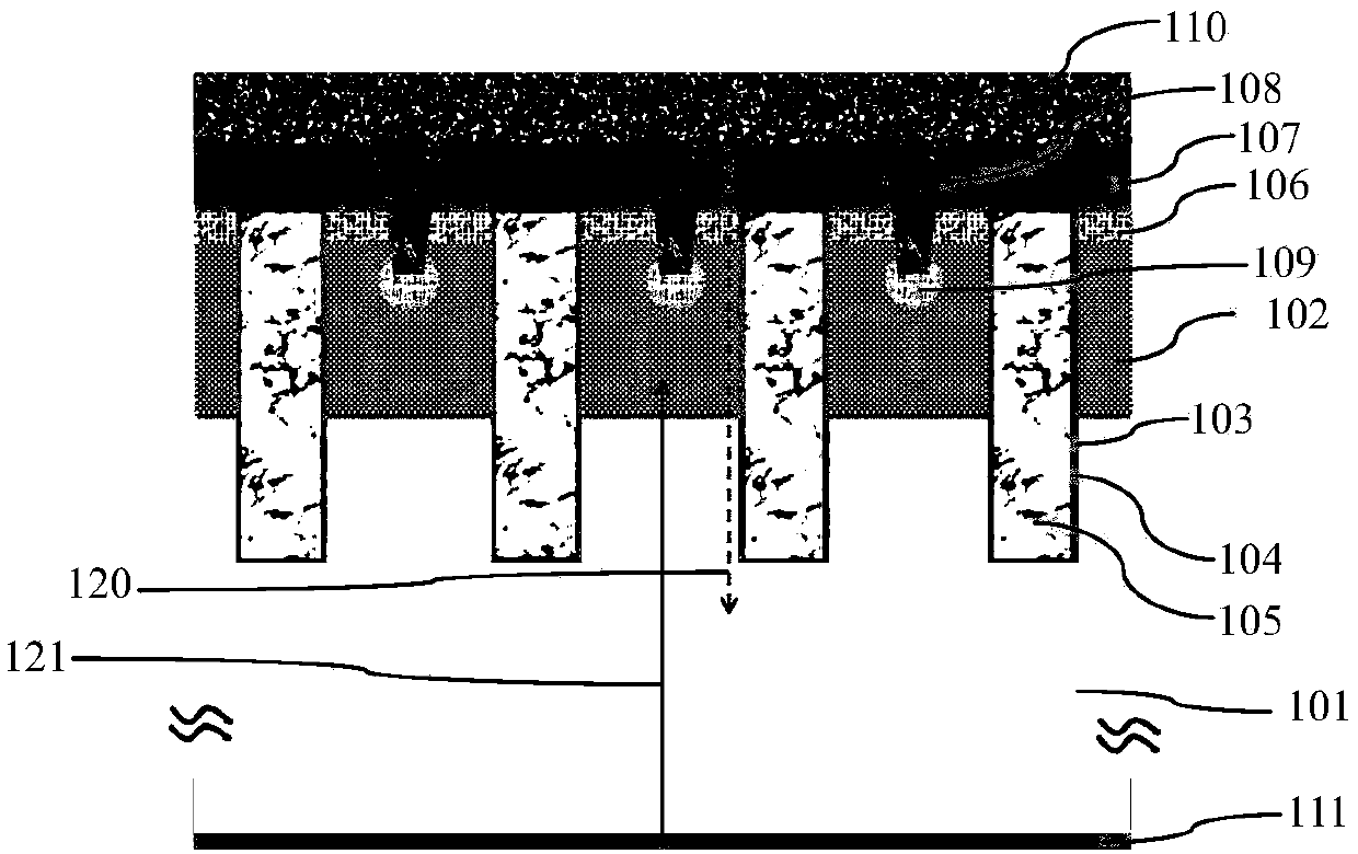
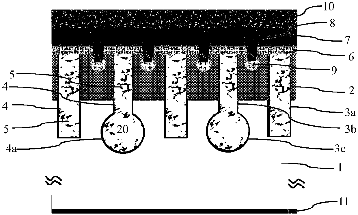
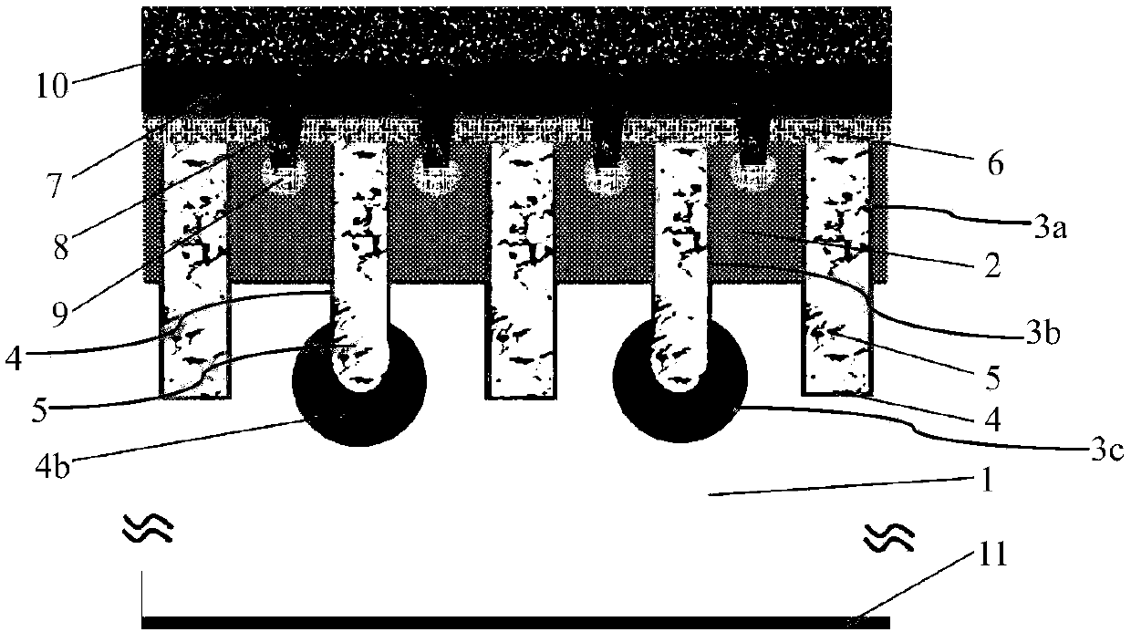
[0067] Such as figure 2 As shown, it is a schematic structural diagram of the carrier storage type IGBT of the first embodiment of the present invention; the carrier storage type IGBT of the first embodiment of the present invention includes:

[0068] The drift region 1 is composed of an N-type lightly doped region formed on the surface of the semiconductor substrate.

[0069] The P-type body region 2 is formed on the surface of the drift region 1 .

[0070] Preferably, the semiconductor substrate is a silicon substrate. A silicon epitaxial layer is formed on the surface of the silicon substrate, the drift region 1 is directly composed of the silicon epitaxial layer lightly doped with N-type, and the P-type body region 2 is formed on the surface of the drift region 1 . In the silicon epitaxial layer.

[0071] A hole injection layer 11 composed of a P+ region is formed on the bottom surface of the drift region 1 .

[0072] A plurality of first grooves 3 a and a plurality o...


PUM


Abstract

The invention discloses a carrier storage type IGBT which comprises a drift area, a P type body area, and a hole injection layer. Multiple first and second grooves are arranged alternately. Each of the second trenches is formed by the longitudinal superposition of a bottom trench and a top trench, and a gate dielectric layer and a polysilicon gate are formed in each of the first and two trenches. The bottom trench of the second trench is formed by using isotropic etching after forming the top trench. The bottom trench allows the coverage areas of the side face of the bottom area and the bottom surface of the second trench to be increased. When a device is conducted, a hole storage layer is formed by an N type accumulation layer formed by a drift area surface covered by the side face and bottom surface of the bottom trench. The invention also discloses a manufacturing method of the carrier storage type IGBT. According to the carrier storage type IGBT and the manufacturing method thereof, the storage effect of a hole at the drift area can be enhanced, the pressure drop and anti-latch performance of the IGBT are improved, and breakdown voltage is not sacrificed.

Description

technical field [0001] The invention relates to the field of manufacturing semiconductor integrated circuits, in particular to a carrier storage type IGBT; the invention also relates to a method for manufacturing the carrier storage type IGBT. Background technique [0002] Insulated Gate Bipolar Transistor (IGBT) is a composite fully-controlled voltage-driven power semiconductor device composed of a bipolar transistor (BJT) and an insulated gate field effect transistor (MOSFET). A giant transistor (Giant Transistor, GTR) that can work at high voltage and high current is also a power transistor; IGTB has the advantages of high input impedance of MOSFET and low conduction voltage drop of GTR. It is very suitable for the conversion system with a DC voltage of 600V and above, such as AC motors, frequency converters, switching power supplies, lighting circuits, traction drives and other fields. [0003] Such as figure 1 Shown is a schematic diagram of the existing IGBT structur...

Claims


Application Information

Patent Timeline
Patent Type & Authority Patents(China)
IPC IPC(8): H01L29/739H01L21/331H01L29/06
CPCH01L29/0684H01L29/66325H01L29/7393
Inventor 柯行飞
Owner SHANGHAI HUAHONG GRACE SEMICON MFG CORP
Why Eureka
Try Eureka