Electrochromic material, preparation method and application thereof, and electrochromic device

A technology of electrochromic materials and electrochromic devices, applied in metal material coating technology, instruments, ion implantation plating, etc., can solve the problems of consuming device life, increased transmittance in colored state, poor memory effect, etc. problem, achieve the effect of improving the memory effect, inhibiting the self-extrusion process, and prolonging the time for maintaining low transmittance

Active Publication Date: 2021-02-02
GUANGDONG INST OF NEW MATERIALS
View PDF7 Cites 0 Cited by
  • Summary
  • Abstract
  • Description
  • Claims
  • Application Information

AI Technical Summary

Problems solved by technology

But for the most widely used WO 3 For the electrochromic layer, the biggest problem is that when the voltage is disconnected after coloring, the transmittance in the colored state will continue to increase, that is, the dark blue color will gradually become lighter, and the memory effect is poor. The direct result is that the WO 3 The electrochromic film is colored twice or more times, which will consume energy and consume the service life of the device

Method used


Image

  • Electrochromic material, preparation method and application thereof, and electrochromic device
  • Electrochromic material, preparation method and application thereof, and electrochromic device
  • Electrochromic material, preparation method and application thereof, and electrochromic device

Examples


preparation example Construction

[0056] In the second aspect, the present application also provides a preparation method of the aforementioned electrochromic material, for example, may include the following steps: depositing WO on the surface of the substrate by means of vacuum magnetron sputtering 3 layer, followed by WO 3 A protective layer is prepared on the surface of the layer facing away from the substrate.

[0057] In an optional embodiment, the protective layer is prepared by vacuum magnetron sputtering.

[0058] In an optional embodiment, WO in this application 3 During the vacuum magnetron sputtering process of the layer, the sputtering power can be 80-120W, such as 80W, 85W, 90W, 95W, 100W, 105W, 110W, 115W or 120W. The sputtering time may be 60-150 min, such as 60 min, 70 min, 80 min, 90 min, 100 min, 110 min, 120 min, 130 min, 140 min or 150 min, etc. Preferably, the sputtering time is 70-130 min.

[0059] It is worth noting that the inventors found that WO 3 If the vacuum magnetron sputterin...

Embodiment 1

[0078] This embodiment provides a kind of WO for electrochromic device 3 / protective layer structure thin film electrochromic layer, which uses SnO 2 As the protective layer material, the substrate is made of ITO transparent conductive glass, and the specific preparation method is as follows:

[0079] An ultra-high vacuum multi-target magnetron sputtering apparatus (JGP-560, Shenyang Scientific Instrument Development Center Co., Ltd., Chinese Academy of Sciences) was used for sputtering, and the sputtering power was 100W. First, WO with a purity of 99.99% 3 with SnO 2 The targets are respectively installed on the target head of the RF power supply; the ITO transparent conductive glass substrate is cleaned in sequence with acetone, absolute ethanol and deionized water in an ultrasonic cleaner to remove oil and dust on the surface of the substrate, and then placed in a vacuum After drying in the drying oven, take it out, install the ITO transparent conductive glass substrate ...

Embodiment 2

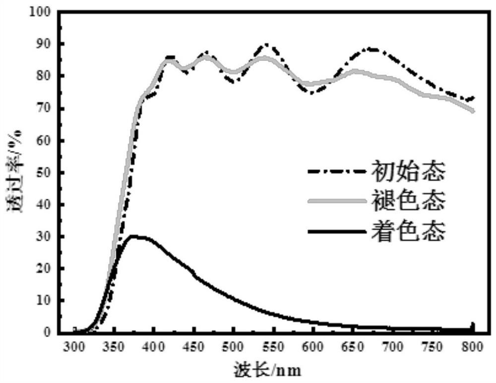
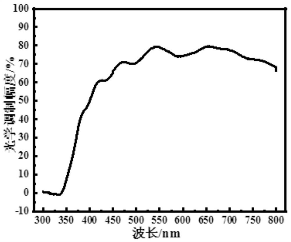
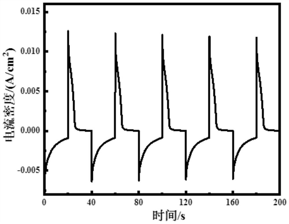
[0085] IFO / WO of this embodiment 3 / SnO 2 The preparation steps of the electrochromic thin film material are basically the same as those described in Example 1, except that the IFO conductive glass is used as the substrate, and the SnO 2 The sputtering time used for the layering of thin films was 10 min. Figure 4 WO prepared for this example 3 / SnO 2 XRD pattern of the structured film.

[0086] WO prepared in this example 3 / SnO 2 The cross-sectional morphology of structural thin film materials is shown in Figure 5 , as shown in the figure, the total thickness of the structured film is about 450nm, where WO 3 The thickness of the active layer is about 350nm, and the upper layer of SnO 2 The thickness of the layer is about 100 nm. At the same time, SnO can be found 2 layer and WO 3 The bonding of the layers is better, which will benefit the SnO 2 layer pair WO 3 Support and protection of active particles, thus improving long-term cycle stability. and SnO 2 The ...


PUM

PropertyMeasurementUnit
thicknessaaaaaaaaaa
thicknessaaaaaaaaaa
thicknessaaaaaaaaaa

Abstract

The invention discloses an electrochromic material, a preparation method and application thereof, and an electrochromic device, and belongs to the technical field of electrochromic device manufacturing. The electrochromic material comprises a WO3 layer used for being deposited on the surface of a substrate and a protective layer arranged on the surface of the WO3 layer, the WO3 layer is prepared in a vacuum magnetron sputtering mode, and the protective layer is prepared from transparent transition metal oxide. The electrochromic material can reduce the color lightening speed of WO3 after coloring, and effectively improves the memory effect of a WO3 electrochromic film. The preparation method comprises the following steps: depositing the WO3 layer on the surface of the substrate in a vacuummagnetron sputtering mode, and then preparing the protective layer on the surface of one side, far away from the substrate, of the WO3 layer. The method is simple in process, has designability and controllability, and is relatively high in flexibility. When the electrochromic material is used in an electrochromic device, the device can cut off voltage after being colored, the transmittance of thecolored state is low, the original color is kept for a long time, and the memory effect is high.

Description

technical field [0001] The invention relates to the technical field of electrochromic device manufacturing, in particular to an electrochromic material, a preparation method and application thereof, and an electrochromic device. Background technique [0002] Electrochromic devices are widely used in daily life because only a small voltage (<1V) is required to complete the change of optical constants such as color and transparency. But for the most widely used WO 3 For the electrochromic layer, the biggest problem is that when the voltage is disconnected after coloring, the transmittance of the colored state will continue to increase, that is, the dark blue will gradually become lighter, and the memory effect is poor. The direct result is that the WO 3 The electrochromic film undergoes secondary or multiple coloring, which consumes energy and consumes the service life of the device. [0003] In view of this, the present invention is proposed. Contents of the invention ...

Claims


Application Information

Patent Timeline
Patent Type & Authority Applications(China)
IPC IPC(8): G02F1/1514G02F1/1524G02F1/153C23C14/08C23C14/35
CPCG02F1/1514G02F1/1524G02F1/1533C23C14/083C23C14/086C23C14/08C23C14/352G02F2001/1536
Inventor 石倩韩文芳胡仁宗王红莉唐春梅林松盛代明江苏一凡唐鹏黄淑琪
Owner GUANGDONG INST OF NEW MATERIALS
Why Eureka
Try Eureka