Avalanche photodiode used for communication and preparation method thereof

A technology of avalanche photodiodes and diodes, which is applied in circuits, electrical components, semiconductor devices, etc., can solve the problems of high cost, difficulty in manufacturing avalanche photodiodes, and low stability, and achieve reduced chip resistance, high stability, and reduced The effect of the circuit time constant

Active Publication Date: 2016-11-09
WUHAN HUAGONG GENUINE OPTICS TECH
View PDF4 Cites 17 Cited by
  • Summary
  • Abstract
  • Description
  • Claims
  • Application Information

AI Technical Summary

Problems solved by technology

[0007] The purpose of the present invention is to provide an avalanche photodiode for communication and its preparation method, aim

Method used


Image

  • Avalanche photodiode used for communication and preparation method thereof

Examples


Embodiment Construction

[0027] The following will clearly and completely describe the technical solutions in the embodiments of the present invention with reference to the accompanying drawings in the embodiments of the present invention. Obviously, the described embodiments are only some, not all, embodiments of the present invention. Based on the embodiments of the present invention, all other embodiments obtained by persons of ordinary skill in the art without making creative efforts belong to the protection scope of the present invention.

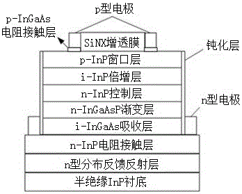
[0028] Such as figure 1 An embodiment of the present invention provides an avalanche photodiode for communication. The epitaxial structure of the avalanche photodiode specifically includes: a semi-insulating InP substrate, an n-type distributed feedback reflection layer, an n-InP resistive contact layer, and an i- InGaAs absorption layer, n-InGaAsP gradient layer, n-InP control layer, i-InP multiplication layer, p-InP window layer, heavily doped p-InGaAs resis...


PUM

PropertyMeasurementUnit
Diameteraaaaaaaaaa

Abstract

The invention provides an avalanche photodiode used for communication and a preparation method thereof. An epitaxial structure of the avalanche photodiode comprises an insulating InP substrate, an n type distribution feedback reflecting layer, an n-InP resistor contact layer, an i-InGaAs absorbing layer, an n-InGaAsP gradient layer, an n-InP control layer, an i-InP multiplication layer, a p-InP window layer, a heavily doped p-InGaAs resistor contact layer and an anti-reflection medium layer, wherein photoetching and etching technologies are utilized to form the vertical normal-incidence avalanche photodiode of a table structure. According to the invention, the avalanche photodiode used for communication meets the high responsivity requirement, the manufacturing is easy, the power consumption is low, and the stability is high.

Description

technical field [0001] The invention relates to an avalanche photodiode for communication, in particular to an avalanche photodiode with high responsivity. Background technique [0002] With the continuous development of the network information industry, the communication between urban areas is getting closer, which means that communication between distant urban areas and long-distance information transmission need to be continuously improved. Therefore, the existing optical transmission rate needs to be continuously improved. Today, there are two types of high-speed optical receivers, one is a PIN photodiode, and the other is an avalanche photodiode (APD). Compared with the PIN principle, APD is a semiconductor optoelectronic with internal photocurrent gain. A device that uses the impact ionization effect of photogenerated carriers in the depletion layer to obtain the avalanche multiplication effect of photocurrent. Therefore, the receiving rate of APD at 2.5Gb / s and 10Gb / ...

Claims


Application Information

Patent Timeline
IPC IPC(8): H01L31/107H01L31/18
CPCH01L31/107H01L31/184
Inventor 刘思思郭明玮
Owner WUHAN HUAGONG GENUINE OPTICS TECH
Why Eureka
Try Eureka