High-quality AlN thin film epitaxially grown on Si substrate, and preparation method of high-quality AlN thin film

An epitaxial growth, high-quality technology, applied in semiconductor/solid-state device manufacturing, electrical components, circuits, etc., can solve the problems of complex growth process, many influencing factors, and long time consumption, and achieve unique growth process, improve mobility, and grow The effect of simple and easy process

Active Publication Date: 2016-11-16
广州市艾佛光通科技有限公司
View PDF3 Cites 13 Cited by
  • Summary
  • Abstract
  • Description
  • Claims
  • Application Information

AI Technical Summary

Problems solved by technology

However, the growth process of this technique is complex, with many influencing factors and time-consuming

Method used


Image

  • High-quality AlN thin film epitaxially grown on Si substrate, and preparation method of high-quality AlN thin film
  • High-quality AlN thin film epitaxially grown on Si substrate, and preparation method of high-quality AlN thin film
  • High-quality AlN thin film epitaxially grown on Si substrate, and preparation method of high-quality AlN thin film

Examples


preparation example Construction

[0028] A method for preparing a high-quality AlN film epitaxially grown on a Si substrate, comprising the following steps:

[0029] 1) Select Si substrate;

[0030] Using Si as the substrate, the Si substrate is easy to obtain, cheap, and easy to produce in large sizes, which is conducive to reducing production costs;

[0031] 2) Epitaxial pre-applied Al layer: epitaxially pre-applied Al layer on the Si substrate;

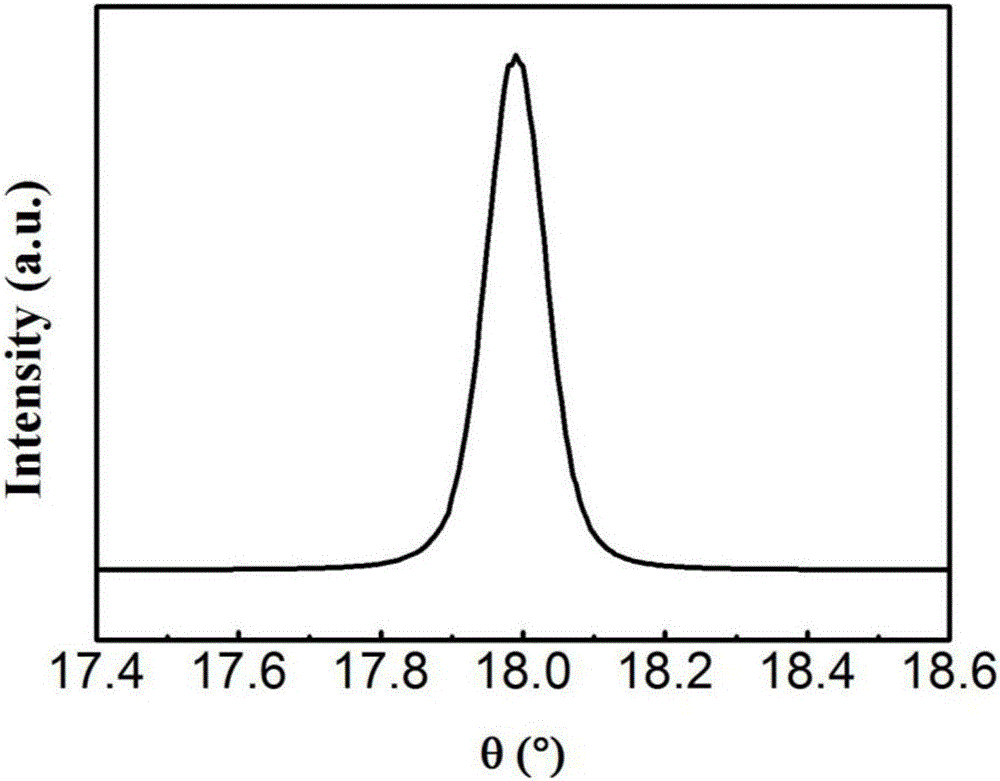
[0032] A layer of Al is pre-laid on the Si substrate to suppress the interface reaction between the Si substrate and the epitaxial layer; then the AlN nucleation layer is grown sequentially to lay the foundation for the further growth of a high-quality AlN film layer, and the obtained The AlN thin film has low dislocation density, small value of half-peak width, and high quality. The method of pre-laying the Al layer includes but is not limited to the use of MOCVD technology;

[0033] 3) Growth of AlN nucleation layer: use NH 3 Carrying out nitriding treatment ...

Embodiment 1

[0037] A method for preparing a high-quality AlN film epitaxially grown on a Si substrate, comprising the following steps:

[0038] 1) Select Si substrate: Si substrate is used, and the epitaxial plane is 0.2-1° away from the (110) direction of the closest-packed plane (111), and the crystal epitaxial orientation relationship is: the (0002) plane of AlN is parallel to that of Si (111) face;

[0039] Surface cleaning and baking of the substrate:

[0040] The specific process of cleaning is: put the Si substrate into H2 mixed with 5% HF 2 SO 4 :H 2 o 2 :H 2 O=3:1:1 ultrasonic cleaning at room temperature in a mixed acid solution for 10-15 seconds to remove the oxide film and organic matter on the surface of the Si substrate, rinse the Si substrate with deionized water, and then ultrasonically wash with deionized water for 1-3 Minutes to remove residual chemical reagents on the surface, and finally blow dry with high-purity dry nitrogen;

[0041] The specific baking proces...

Embodiment 2

[0047] A method for preparing a high-quality AlN film grown on a Si substrate, comprising the following steps:

[0048] 1) Select Si substrate: Si substrate is used, and the epitaxial plane is 0.2-1° away from the (110) direction of the closest-packed plane (111), and the crystal epitaxial orientation relationship is: the (0002) plane of AlN is parallel to that of Si (111) face;

[0049] The specific process of cleaning is: put the Si substrate into H2 mixed with 5% HF 2 SO 4 :H 2 o 2 :H 2 O=3:1:1 ultrasonic cleaning at room temperature in a mixed acid solution for 10-15 seconds to remove the oxide film and organic matter on the surface of the Si substrate, rinse the Si substrate with deionized water, and then ultrasonically wash with deionized water for 1-3 Minutes to remove residual chemical reagents on the surface, and finally blow dry with high-purity dry nitrogen;

[0050] The specific process of baking is as follows: put the substrate into the MOCVD reaction chambe...


PUM

PropertyMeasurementUnit
thicknessaaaaaaaaaa
thicknessaaaaaaaaaa

Abstract

The invention discloses a high-quality AlN thin film epitaxially grown on a Si substrate, and a preparation method of the high-quality AlN thin film. The preparation method specifically comprises the following steps of 1) choosing the Si substrate; 2) pre-paving an Al layer in an epitaxial manner; 3) enabling an AlN core-forming layer to be grown; and 4) enabling the AlN thin film to be grown, wherein in the growth process of the AlN thin film, trimethyl gallium is introduced at a speed of 0.2-0.5mL/min to be used as a surfactant. By adoption of the preparation method, the relatively thick and crack-free AlN thin film with a thickness which is greater than 1[mu]m can be manufactured; inter-island union and two-dimensional growth of the AlN thin film are realized; compared with a multi-step multi-layered or high-temperature AlN thin film growth technology, the time consumption for preparing the thin film by the method provided by the invention can be shortened; the growth process is unique, simple and feasible; the large-scale production can be realized conveniently; and the thin film can be widely applied to the fields of a photovoltaic thin film for an LED, an ultraviolet and deep ultraviolet device, a surface acoustic wave device and the like.

Description

technical field [0001] The invention relates to the technical field of AlN thin films, in particular to a high-quality AlN thin film epitaxially grown on a Si substrate and a preparation method thereof. Background technique [0002] AlN is an important III-V compound semiconductor material with low thermal expansion coefficient, excellent mechanical strength, high electrical insulation properties, wide band gap and high surface acoustic wave velocity, these characteristics make AlN in mechanical, Optics, electronic components, surface acoustic wave device manufacturing and other fields have broad application prospects. In addition, AlN also has good stability, high thermal conductivity, similar lattice constant and thermal expansion coefficient to GaN and AlGaN, so AlN has become a preferred material for GaN and AlGaN buffer layers, which can effectively improve the nitride epitaxy. The crystalline quality of the film significantly improves its photoelectric performance. ...

Claims


Application Information

Patent Timeline
Patent Type & Authority Applications(China)
IPC IPC(8): H01L21/02
CPCH01L21/02381H01L21/0254H01L21/0262
Inventor 李国强
Owner 广州市艾佛光通科技有限公司
Why Eureka
Try Eureka