Method for preparing thick epitaxial layer on thin sb substrate for VDMOS device

A substrate and epitaxy technology, which is applied in the field of silicon epitaxial layer preparation process for VDMOS devices, can solve the problems of increased epitaxial debris rate, chipping, slip line, and increased difficulty in controlling the uniformity of epitaxial thickness, etc., to improve processing quality. High rate, good uniformity of thickness, and good quality of edge crystallization

Active Publication Date: 2016-11-16
CHINA ELECTRONICS TECH GRP NO 46 RES INST +1
View PDF3 Cites 17 Cited by
  • Summary
  • Abstract
  • Description
  • Claims
  • Application Information

AI Technical Summary

Problems solved by technology

But at the same time, due to the reduction of the substrate thickness, the epitaxial growth fluid model and crystal stress distribution will be different, and the uniformity of the epitaxial thickness and the difficulty of defect control will be greatly increased. In view of the fact that the growth rate of the epitaxial edge is higher than that of the center, When growing thick epitaxy, due to the long growth time and the continuous accumulation of extrusion stress caused by thermal history, it is very easy to have defects such as "epitaxial crown", chipping, and slip lines on the edge of the epitaxy. In the subsequent device process , the edge cracks continue to expand and extend, resulting in a large increase in the rate of epitaxial fragmentation, especially the stress and damage problems on the main reference edge are more prominent, which has an extremely adverse impact on subsequent device process equipment and process control

Method used


Image

  • Method for preparing thick epitaxial layer on thin sb substrate for VDMOS device
  • Method for preparing thick epitaxial layer on thin sb substrate for VDMOS device
  • Method for preparing thick epitaxial layer on thin sb substrate for VDMOS device

Examples


Embodiment 1

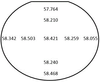
[0022] Step 1: The bottom end of the induction coil under the graphite base of the epitaxial furnace has 9 sets of distance-adjustable adjustment rods, named 4#~12# respectively. By rotating the adjustment rods to lift or pull down the position of the coil, adjust the coil The distance between each part and the graphite base can improve the temperature uniformity of the base. The scale value of the 4# adjustment rod is set to -10, the scale value of the 5# adjustment rod is set to -15, and the scale value of the 6# adjustment rod is set to -15. The scale value of the lever is set to -30, the scale value of the 7# adjusting lever is set to -30, the scale value of the 8# adjusting lever is set to 0, the scale value of the 9# adjusting lever is set to -30, 10# The scale value of the adjustment rod is set to -30, the scale value of the 11# adjustment rod is set to +3, and the scale value of the 12# adjustment rod is set to +3.

[0023] The second step: use hydrogen chloride (HCl) ...

Embodiment 2

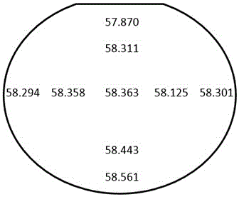
[0032] Step 1: The bottom end of the induction coil under the graphite base of the epitaxial furnace has 9 sets of distance-adjustable adjustment rods, named 4#~12# respectively. By rotating the adjustment rods to lift or pull down the position of the coil, adjust the coil The distance between each part and the graphite base can improve the temperature uniformity of the base. The scale value of the 4# adjustment rod is set to -8, the scale value of the 5# adjustment rod is set to -13, and the scale value of the 6# adjustment rod is set to -13. The scale value of the lever is set to -28, the scale value of the 7# adjusting lever is set to -28, the scale value of the 8# adjusting lever is set to +2, the scale value of the 9# adjusting lever is set to -29, 10 The scale value of the #adjusting lever is set to -30, the scale value of the 11# adjusting lever is set to +2, and the scale value of the 12# adjusting lever is set to +2.

[0033] Step 2: Use hydrogen chloride gas (HCl) to...

Embodiment 3

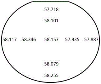
[0042] Step 1: The bottom end of the induction coil under the graphite base of the epitaxial furnace has 9 sets of distance-adjustable adjustment rods, named 4#~12# respectively. By rotating the adjustment rods to lift or pull down the position of the coil, adjust the coil The distance between each part and the graphite base can improve the temperature uniformity of the base. The scale value of the 4# adjustment rod is set to -7, the scale value of the 5# adjustment rod is set to -13, and the scale value of the 6# adjustment rod is set to -13. The scale value of the lever is set to -28, the scale value of the 7# adjusting lever is set to -30, the scale value of the 8# adjusting lever is set to +2, the scale value of the 9# adjusting lever is set to -27, 10# Set the scale value of the adjustment lever to -27, set the scale value of the 11# adjustment lever to +1, and set the scale value of the 12# adjustment lever to +1;

[0043] Step 2: Use hydrogen chloride (HCl) to polish th...


PUM

PropertyMeasurementUnit
thicknessaaaaaaaaaa

Abstract

The invention relates to a method for preparing a thick epitaxial layer on a thin sb substrate for a VDMOS device. The method comprises: scale values of nine groups of adjusting rods arranged below a graphite pedestal of an epitaxial furnace are set respectively; the epitaxial furnace pedestal is processed by etching and polishing by using hydrogen chloride HC1 gas under a high temperature; a silicon substrate sheet is installed in a pit of the epitaxial furnace pedestal and the surface of the silicon substrate is polished by using the HC1 gas; sweeping is carried out on the surface of the silicon substrate sheet by using high-flow hydrogen; a thin intrinsic epitaxial layer grows on the silicon substrate sheet; a doped epitaxial layer grows; after the thickens of the doped epitaxial layer reaches a predetermined thickness, cooling is carried out; and then thicknesses of nine testing points of the epitaxial wafer are measured, thereby obtaining an average thickness value and a uniformity value of a silicon epitaxial wafer. Therefore, good control of epitaxial growth of the thin 400-micron sb substrate is realized; the nonuniformity of the thickness is less than 0.5%; defects of slip line, edge breakage, and damage existence at the edge are overcome; and the requirements on the silicon epitaxial layer of the VDMOS device are met; and the processing yield of the device is improved.

Description

technical field [0001] The invention relates to a preparation technology of a silicon epitaxial layer for a VDMOS device, in particular to a method for preparing a thick layer epitaxy on a thin Sb substrate for a VDMOS device. Background technique [0002] VDMOS power device is a kind of semiconductor device with high input impedance, good thermal stability, low power consumption and fast switching speed. Applications. VDMOS devices use a multi-cell structure in which hundreds or thousands of repeated MOS units are connected in parallel to achieve greater operating current, and the quality of a single cell directly determines the performance of the device. The base material mainly adopts N-type Sb-doped silicon <100> crystal-oriented back-sealing substrate, and the good electrical characteristics of the cells require that the epitaxial material has better uniformity and lower defect density. [0003] In order to reduce the cost of chips, 6-inch silicon epitaxial wafe...

Claims


Application Information

Patent Timeline
Patent Type & Authority Applications(China)
IPC IPC(8): H01L21/02
CPCH01L21/02538H01L21/0262
Inventor 陈涛李明达薛兵白春磊殷海丰
Owner CHINA ELECTRONICS TECH GRP NO 46 RES INST
Why Eureka
Try Eureka