

Superconducting nanowire single photon detector fabricated on micro-nano fiber surface
A single-photon detector and superconducting nanowire technology, applied in the field of light detection, can solve problems such as low detection efficiency, and achieve the effects of improving optical coupling efficiency, reducing dynamic inductance, and improving speed.
- Summary
- Abstract
- Description
- Claims
- Application Information
AI Technical Summary
Problems solved by technology
Method used
Image

Examples
Embodiment 1
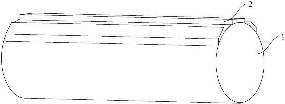
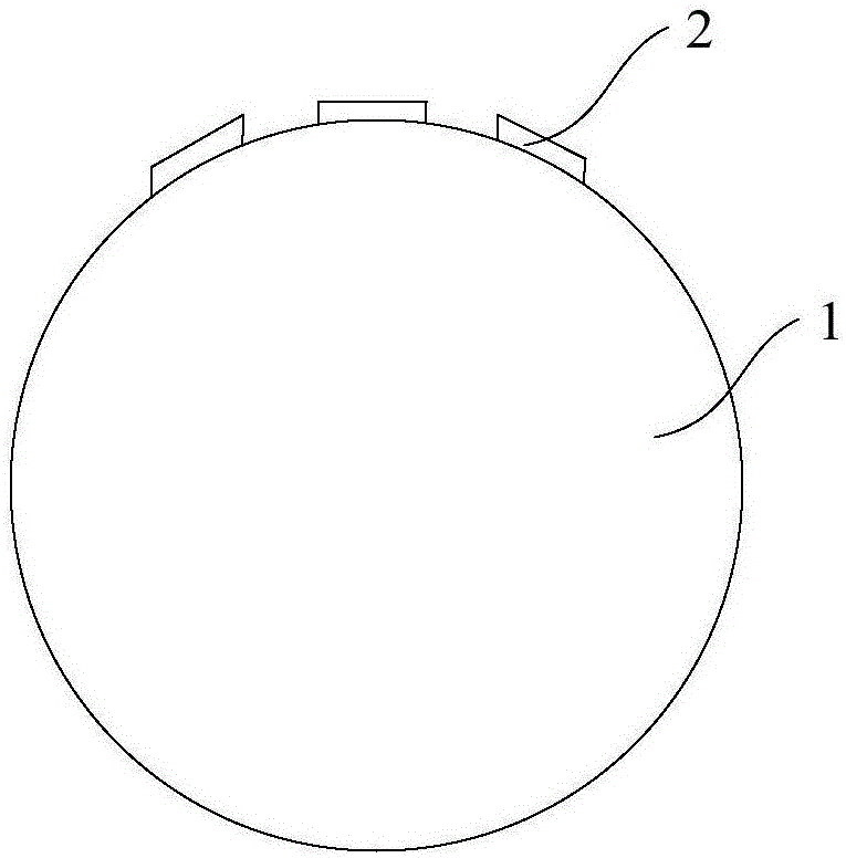
[0029] see figure 1 and figure 2 , the present invention provides a superconducting nanowire single-photon detector prepared on the surface of a micro-nano fiber. The superconducting nano-wire single-photon detector prepared on the surface of a micro-nano fiber includes: a micro-nano fiber 1 and a superconducting nanowire 2; Wherein, the superconducting nanowire 2 is located on the surface of the micro-nano fiber 1 , and the length direction of the superconducting nanowire 2 is consistent with the length direction of the micro-nano fiber 1 .
[0030] As an example, the micro-nano fiber 1 is drawn from a standard single-mode fiber, and the material of the micro-nano fiber 1 is SiO 2 .
[0031] As an example, the shape of the micro-nano fiber 1 is a cylindrical conical shape, and the diameter of the end face of the micro-nano fiber 1 is 1 micron, that is, the diameter of the cross-section of the micro-nano fiber 1 is 1 micron; The optical transmittance of the optical fiber 1...
Embodiment 2
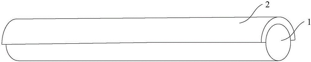
[0041] see image 3 and Figure 4 , the present invention also provides a superconducting nanowire single-photon detector prepared on the surface of the micro-nano fiber, the superconducting nano-wire single-photon detector prepared on the surface of the micro-nano fiber is the same as the surface of the micro-nano fiber described in Embodiment 1 The structure of the prepared superconducting nanowire single photon detector is basically the same, the difference between the two is: the diameter of the micro-nano fiber 1 in the first embodiment is 1 micron, and the number of the superconducting nanowire 2 is 3 , the preparation method of the superconducting nanowire 2 is to use the magnetron sputtering process to form the NbN superconducting film and then need to etch the process; and in the present embodiment, the diameter of the micro-nano fiber 1 is 0.1 micron, so The root number of the superconducting nanowires is 1, and the preparation method of the superconducting nanowire...
PUM
| Property | Measurement | Unit |
|---|---|---|
| Diameter | aaaaa | aaaaa |
| Length | aaaaa | aaaaa |
| Thickness | aaaaa | aaaaa |
Abstract
Description
Claims
Application Information