Method for preparing micro-fluidic chip template

A microfluidic chip and template technology, applied in the field of micro-manufacturing, can solve the problems of long processing time cycle, short processing time cycle, and high processing technology cost, and achieve the effects of low cost, low production cost, and shortened processing cycle

Inactive Publication Date: 2016-11-23
HUAZHONG UNIV OF SCI & TECH
View PDF3 Cites 10 Cited by
  • Summary
  • Abstract
  • Description
  • Claims
  • Application Information

AI Technical Summary

Problems solved by technology

[0010] In short, the existing processing technologies of various microfluidic chips generally have the situation that the accuracy, cost and processing cycle cannot be balanced
The cost of high

Method used


Image

  • Method for preparing micro-fluidic chip template
  • Method for preparing micro-fluidic chip template
  • Method for preparing micro-fluidic chip template

Examples


preparation example Construction

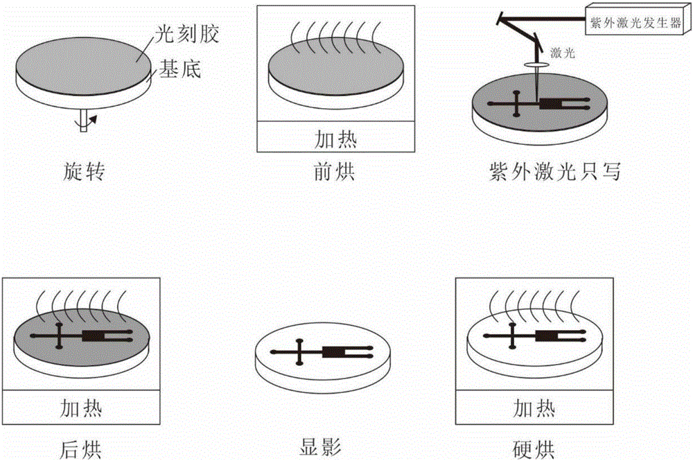
[0035] figure 1 It is a flowchart of the preparation method of the microfluidic chip template in Example 1 of the present invention, such as figure 1 As shown, it mainly includes the following steps:

[0036] S1: Firstly, spin-coat a layer of negative photoresist SU-8 (manufactured by MicroChem, USA) on the silicon wafer with a homogenizer. According to the nature of the photoresist, adjust the speed of the homogenizer to obtain the required Thickness of the photoresist, the thickness of the photoresist is 50 μm.

[0037] S2: According to the properties of the photoresist and the thickness of the spin coating, place it on a heating platform at 60-70°C for 5 minutes, and then place it on a heating plate at 90-100°C. Baking time Carry out pre-baking treatment, and the pre-baking time is 10-20min.

[0038] S3: When the photoresist is cooled to room temperature, the designed pattern is sent to the ultraviolet laser, and the ultraviolet laser is used for selective pattern exposu...

Embodiment 2

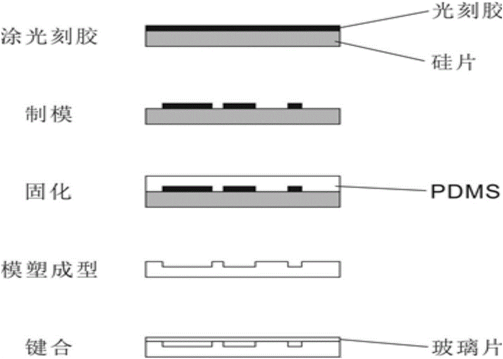
[0046] S1: Firstly, spin-coat a layer of positive photoresist AZ1505 (manufactured by MicroChemicals, UK) on the glass with a homogenizer. According to the nature of the photoresist, adjust the speed of the homogenizer to obtain the required thickness of photoresist , the thickness of the photoresist is 1 micron, and the photoresist is a positive resist.

[0047] S2: According to the properties of the photoresist and the thickness of the spin coating, place it on a heating plate at 95-105°C, select an appropriate pre-baking time for pre-baking treatment, and the pre-baking time is 40-60 seconds.

[0048] S3: When the photoresist is cooled to room temperature, the designed pattern is sent to the ultraviolet laser, and the ultraviolet laser is used for selective exposure, and the laser spot will scan the designed pattern on the photoresist.

[0049] S4: After the photoresist is cooled to room temperature, the photoresist is developed with a developer to obtain a microfluidic chi...

Embodiment 3

[0051] S1: First spin coat a layer of negative photoresist SU-8 (manufactured by MicroChem, USA) on the quartz with a homogenizer. According to the properties of the photoresist, adjust the speed of the homogenizer to obtain the desired thickness. Photoresist, the thickness of the photoresist is 100 microns.

[0052] S2: According to the properties of the photoresist and the thickness of the spin coating, first place it on a heating plate at 60-70°C for 3-5 minutes, then place it on a heating plate at 90-100°C, and select an appropriate pre-baking time for pre-baking For processing, the pre-baking time is 20-30min.

[0053] S3: When the photoresist is cooled to room temperature, the designed pattern is sent to the ultraviolet laser, and the ultraviolet laser is used for selective exposure, and the laser spot will scan the designed pattern on the photoresist.

[0054] S4: In order to fully react the photoresist after exposure to obtain better performance, first place it on a h...


PUM


Abstract

The invention discloses a method for preparing a micro-fluidic chip template. The method comprises the following steps that S1, photoresist is used for coating a plane substrate, and the coating thickness of the photoresist is 1 micron to 100 microns; S2, the photoresist coating the plane substrate is subjected to prebaking treatment for volatilizing solvents inside the photoresist, so that the photoresist is cured, and the surface becomes flat; S3, a designed pattern of the micro-fluidic chip template is sent to an ultraviolet laser; ultraviolet laser light is focused into a beam of light spot in the laser; according to the designed pattern, the light spot is driven to move for directly performing exposure on the photoresist covering the substrate in the step S2; S4, the unnecessary photoresist is cleaned away, and the micro-fluidic chip template is obtained. The method has the advantage that through a laser direct writing technique and a photoetching technique, the micro-fluidic chip template is fast and flexibly processed, so that the chip processing cost can be effectively reduced; the chip processing period is shortened.

Description

technical field [0001] The invention relates to microfluidic control manufacturing technology, which belongs to the field of micromanufacturing technology, in particular to a method for quickly and flexibly preparing a microfluidic chip template. Background technique [0002] Microfluidics is widely used in biological detection, chemical analysis, medical detection, environmental engineering, food engineering and other fields that are closely related to our lives. As a new technology, microfluidics also has many applications in the field of scientific research. In the actual research and development process, it is necessary to repeatedly verify and modify the design of the microfluidic chip. [0003] Soft lithography is the most widely used microfluidic chip fabrication technology today. The soft etching technology first needs to manufacture the corresponding template, and then replicate the microstructure on the template through the elastomer. Many methods for manufactur...

Claims


Application Information

Patent Timeline
IPC IPC(8): G03F7/00
CPCG03F7/00G03F7/002
Inventor 吴志刚刘振华徐文超张硕彭鹏张攀邓杰
Owner HUAZHONG UNIV OF SCI & TECH
Why Eureka
Try Eureka