LED epitaxy structure capable of improving GaN crystal quality
A technology of epitaxial structure and crystal quality, which is applied in the direction of semiconductor devices, electrical components, circuits, etc., can solve the problems that cannot effectively overcome the lattice mismatch, reduce the carrier confinement ability of quantum wells, and reduce the recombination probability
- Summary
- Abstract
- Description
- Claims
- Application Information
AI Technical Summary
Problems solved by technology
Method used
Image

Examples
Embodiment 1
[0020] The growth method of the LED epitaxial structure of the present invention is:
[0021] 1) The device is baked at a high temperature in an MOCVD reactor to remove residual impurities on the surface of the patterned substrate 1 .
[0022] 2) Slowly lower the temperature between 400-800°C, and grow a layer of GaN buffer layer 2 on the patterned substrate 1.
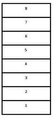
[0023] 3) Raise the temperature rapidly, at 1000-1200°C, grow a U1-type GaN layer 3 on the GaN buffer layer 2, grow for 5-50min, and have a thickness of 0.5-5um.
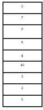
[0024] 4) Re-grow a U2-type GaN layer 40 on the U1-type GaN layer 3:
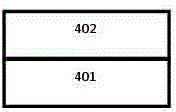
[0025] a) First grow a 2D-type GaN layer 401 at a growth temperature of 1050° C., a thickness of 0.05 μm, and a growth pressure of 100 torr;
[0026] b) Then grow the 3D GaN layer 402 by rapid cooling and pressurization, the growth temperature is 990°C, the growth thickness is 0.05um, and the growth pressure is 400torr;
[0027] c) The growth cycle of the U2-type GaN layer 40 for impr...
Embodiment 2
[0034] The growth method of the LED epitaxial structure of the present invention is:
[0035] 1) The device is baked at a high temperature in an MOCVD reactor to remove residual impurities on the surface of the patterned substrate 1 .
[0036] 2) Slowly lower the temperature between 400-800°C, and grow a layer of GaN buffer layer 2 on the patterned substrate 1.
[0037] 3) Raise the temperature rapidly, at 1000-1200°C, grow a U1-type GaN layer 3 on the GaN buffer layer 2, grow for 5-50min, and have a thickness of 0.5-5um.
[0038] 4) Re-grow a U2-type GaN layer 40 on the U1-type GaN layer 3:
[0039]a) First grow a 2D GaN layer 401 at a growth temperature of 1080°C, a thickness of 0.1um, and a growth pressure of 200torr;
[0040] b) Then grow the 3D GaN layer 402 by rapid cooling and pressurization, the growth temperature is 1020°C, the growth thickness is 0.1um, and the growth pressure is 500torr;
[0041] c) The growth cycle of the U2-type GaN layer 40 for improving GaN c...
Embodiment 3
[0048] The growth method of the LED epitaxial structure of the present invention is:
[0049] 1) The device is baked at a high temperature in an MOCVD reactor to remove residual impurities on the surface of the patterned substrate 1 .
[0050] 2) Slowly lower the temperature between 400-800°C to grow a layer of GaN buffer layer 2.
[0051] 3) Raise the temperature rapidly, between 1000-1200°C, grow a U1-type GaN layer 3 on the GaN buffer layer 2, grow for 5-50min, and have a thickness of 0.5-5um.
[0052] 4) Growing U2-type GaN layer 40:
[0053] a) First grow a 2D GaN layer 401 at a growth temperature of 1110°C, a thickness of 0.5um, and a growth pressure of 300torr;
[0054] b) Then grow the 3D GaN layer 402 by rapid cooling and pressurization, the growth temperature is 1050°C, the growth thickness is 0.5um, and the growth pressure is 650torr;
[0055] c) The growth period of the U2-type GaN layer for improving GaN crystal quality is 3 periods.
[0056] 5) N-type GaN lay...
PUM
 Abstract
Description
Claims
Application Information
 - R&D
- Intellectual Property
- Life Sciences
- Materials
- Tech Scout
- Unparalleled Data Quality
- Higher Quality Content
- 60% Fewer Hallucinations
Browse by: Latest US Patents, China's latest patents, Technical Efficacy Thesaurus, Application Domain, Technology Topic, Popular Technical Reports.
© 2025 PatSnap. All rights reserved.Legal|Privacy policy|Modern Slavery Act Transparency Statement|Sitemap|About US| Contact US: help@patsnap.com