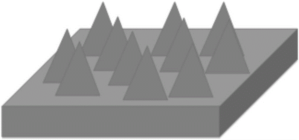
Ceramic micro-needle crystal plate and preparation method thereof
A ceramic micro- and needle-crystal technology is applied in the field of medical beauty equipment, which can solve the problems of insufficient morphology consistency of mesh silicon micro-needles, insufficient micro-needle strength, unsatisfactory puncture effect, poor biocompatibility, etc., and achieves stable and reliable preparation methods. The effect of high drug absorption efficiency and good processing performance
- Summary
- Abstract
- Description
- Claims
- Application Information
AI Technical Summary
Problems solved by technology
Method used
Image
Examples
Embodiment 1
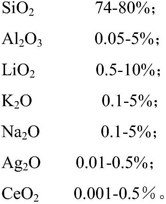
[0038] Prepare ceramic microneedle wafer raw material oxide powder, this powder is made up of the following components by mass percentage:
[0039]
[0040] Prepare ceramic microneedle wafers as follows:
[0041] 1) Prepare a stainless steel mother board, cut the mother board into a rectangle and etch the surface of the mother board to obtain an array of inverted conical needle-shaped depressions, the diameter of the conical bottom surface is 150 μm, and the distance between the centers of the bottom surface is 300 μm;
[0042] 2) mixing the prepared wafer raw materials, and finally coating the raw material mixture on the surface of the motherboard;
[0043] 3) Sintering the raw material mixture at 900°C to obtain a wafer;
[0044] 4) Separate the motherboard and the wafer, and cut the wafer to the required size.
[0045] The thickness of the obtained microneedle wafer is 250 μm, and there are microneedles distributed in an array on the surface. and the spacing between t...
Embodiment 2
[0047] Prepare ceramic microneedle wafer raw material oxide powder, this powder is made up of the following components by mass percentage:
[0048]
[0049] Prepare ceramic microneedle wafers as follows:
[0050]1) Prepare a stainless steel mother board, cut the mother board into a rectangle and etch the surface of the mother board to obtain an array of inverted conical needle-shaped depressions, the diameter of the conical bottom surface is 120 μm, and the distance between the centers of the bottom surface is 200 μm;
[0051] 2) mixing the prepared wafer raw materials, and finally coating the raw material mixture on the surface of the motherboard;
[0052] 3) Sintering the raw material mixture at 1200°C to obtain a wafer;
[0053] 4) Separate the motherboard and the wafer, and cut the wafer to the required size.
[0054] The thickness of the obtained microneedle wafer is 450 μm, and there are microneedles distributed in an array on the surface. and the spacing between t...
Embodiment 3
[0056] Prepare ceramic microneedle wafer raw material oxide powder, this powder is made up of the following components by mass percentage:
[0057]
[0058] Prepare ceramic microneedle wafers as follows:
[0059] 1) Prepare a stainless steel mother board, cut the mother board into a rectangle and etch the surface of the mother board to obtain an array of inverted conical needle-shaped depressions, the diameter of the conical bottom surface is 120 μm, and the distance between the centers of the bottom surface is 300 μm;
[0060] 2) mixing the prepared wafer raw materials, and finally coating the raw material mixture on the surface of the motherboard;
[0061] 3) Sintering the raw material mixture at 1100°C to obtain a wafer;
[0062] 4) Separate the motherboard and the wafer, and cut the wafer to the required size.
[0063] The thickness of the obtained microneedle wafer is 450 μm, and there are microneedles distributed in an array on the surface. The pitch between the ne...
PUM
| Property | Measurement | Unit |
|---|---|---|
| height | aaaaa | aaaaa |
| diameter | aaaaa | aaaaa |
| diameter | aaaaa | aaaaa |
Abstract
Description
Claims
Application Information


