A high-frequency horizontal double-diffused oxide semiconductor device and its manufacturing method

An oxide semiconductor and double-diffusion technology, which is applied in semiconductor/solid-state device manufacturing, semiconductor devices, semiconductor/solid-state device components, etc. The effects of grid defects, reduced on-resistance, and simple process

Active Publication Date: 2019-08-06
FOUNDER MICROELECTRONICS INT
View PDF5 Cites 0 Cited by
  • Summary
  • Abstract
  • Description
  • Claims
  • Application Information

AI Technical Summary

Problems solved by technology

Although sinking ion drive would reduce this effect, there is still a risk
This risk makes the on-resistance of the device unstable and tends to be large

Method used


Image

  • A high-frequency horizontal double-diffused oxide semiconductor device and its manufacturing method
  • A high-frequency horizontal double-diffused oxide semiconductor device and its manufacturing method
  • A high-frequency horizontal double-diffused oxide semiconductor device and its manufacturing method

Examples


Embodiment Construction

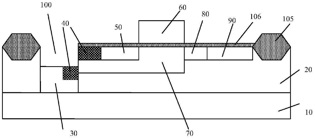
[0033] Embodiments of the present invention will be described in detail below with reference to the accompanying drawings.

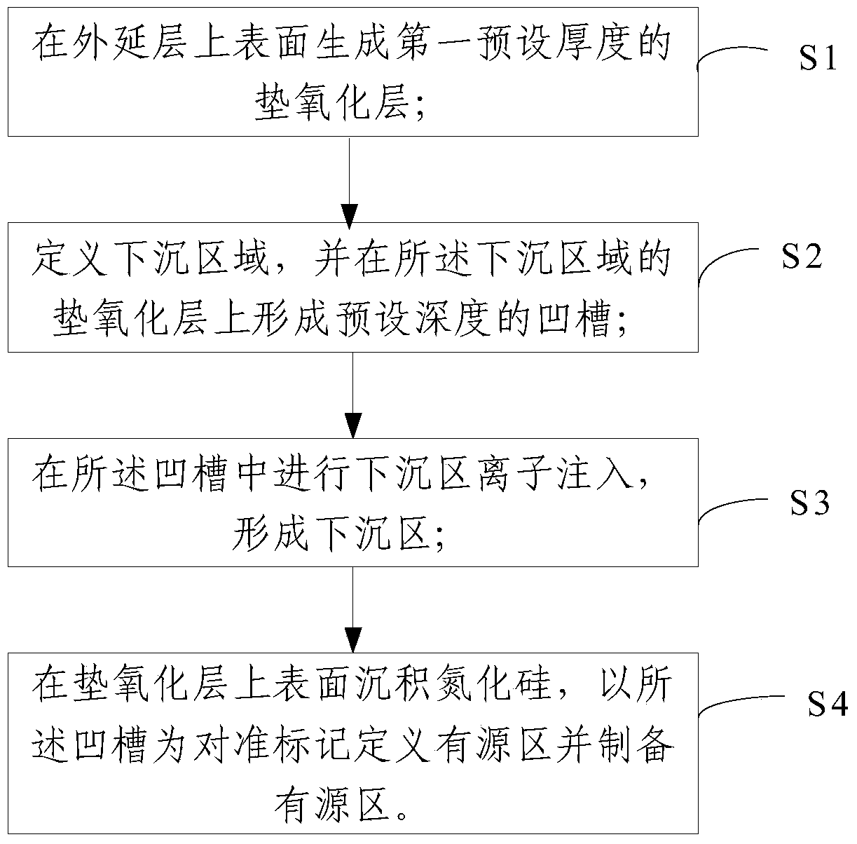
[0034] figure 2 A flow chart of the method of fabricating an RF LDMOS device of the present invention is shown.

[0035] refer to figure 2 , the concrete process of the method for manufacturing RF LDMOS device of the present invention is as follows:

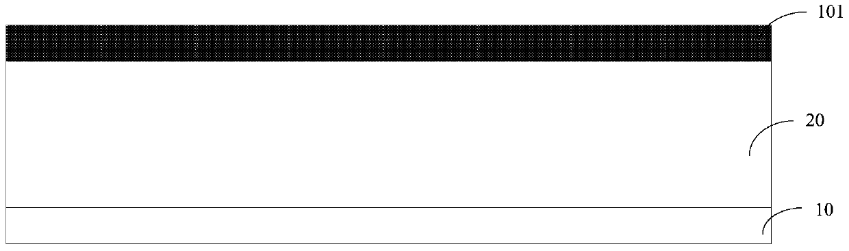
[0036] S1, generating a pad oxide layer with a first preset thickness on the upper surface of the epitaxial layer;

[0037] The pad oxide layer in this embodiment is formed by thermally oxidizing the upper surface of the epitaxial layer to form a pad oxide layer of the first preset thickness on the upper surface of the epitaxial layer; or using a chemical vapor deposition process on the epitaxial layer A pad oxide layer with a first preset thickness is deposited on the upper surface of the pad oxide layer, and the thickness of the generated pad oxide layer is 1500-2000 angstroms.

[0038] S2. A first ...


PUM


Abstract

The invention relates to a high-frequency horizontal double diffusion oxide semiconductor device and a manufacturing method thereof. The method comprises the steps that a pad oxide layer with a first preset thickness is generated on the upper surface of an epitaxial layer; a sinking area is defined in a first default area on the pad oxide layer and a groove with a preset depth is formed in the pad oxide layer in the sinking area; the bottom part of the groove is located in the oxide layer; sinking area ion implantation is carried out in the groove to form the sinking area; and silicon nitride is deposited on the upper surface of the pad oxide layer and then an active region is defined by employing the groove as an alignment mark and is prepared. The relatively thick oxide layer is formed on the epitaxial layer, the groove is formed in the oxide layer through etching, and the groove is taken as the alignment mark of forming a sinking layer, so that a fault is prevented from being formed in an ion implantation area in a traditional technology; the on resistance of the device is reduced; and the lattice defect is avoided.

Description

technical field [0001] The invention relates to the technical field of semiconductor devices, in particular to a high-frequency horizontal double-diffused oxide semiconductor device and a manufacturing method thereof. Background technique [0002] High-frequency horizontal double-diffused metal-oxide semiconductor (RF LDMOS) is widely used in mobile phone base stations, radio and television and radar and other fields. Such as figure 1 As shown, the existing N-type RF LDMOS process generally includes preparing a P sinker layer 30, a source layer 50, a polysilicon layer 60, a body region layer 70, a drift layer 80, a drain layer 90, and a P+ layer on a P-type epitaxial layer 20. Injection layer 40 etc. The working principle of the RF LDMOS device is that the sinker layer 30 is connected to the source layer 50 through the P+ injection layer 40, and the P+ injection layer 40 and the source layer are short-circuited through the metal of the contact hole. After the channel unde...

Claims


Application Information

Patent Timeline
Patent Type & Authority Patents(China)
IPC IPC(8): H01L29/78H01L21/336H01L23/544
Inventor 闻正锋邱海亮马万里赵文魁
Owner FOUNDER MICROELECTRONICS INT
Why Eureka
Try Eureka