Optical dielectric film passivation-based vertical cavity surface laser and preparation method therefor

An optical medium, vertical cavity surface technology, applied in lasers, laser parts, semiconductor lasers, etc., can solve the problems of increasing chip manufacturing costs, the chip performance is deeply affected by the process, and increasing the complexity of the process. The effect of reducing production costs and reducing error damage

Active Publication Date: 2016-12-07
GUANGXUN SCI & TECH WUHAN +1
View PDF4 Cites 0 Cited by
  • Summary
  • Abstract
  • Description
  • Claims
  • Application Information

AI Technical Summary

Problems solved by technology

[0004] In order to improve the performance of the laser, optimizing the laser from many aspects will undoubtedly increase the complexity of the process
The more complex the process, the more deeply the performance of the chip is affected by the process, and the more complex the process, the higher the production cost of the chip.

Method used


Image

  • Optical dielectric film passivation-based vertical cavity surface laser and preparation method therefor
  • Optical dielectric film passivation-based vertical cavity surface laser and preparation method therefor
  • Optical dielectric film passivation-based vertical cavity surface laser and preparation method therefor

Examples


Embodiment 1

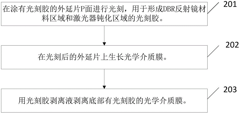
[0084] An embodiment of the present invention provides a method for fabricating a vertical cavity surface laser based on optical dielectric film passivation, such as figure 1 As shown, the preparation method specifically includes the following steps:

[0085] In step 201, photolithography is performed on the surface P of the epitaxial wafer coated with photoresist to etch the photoresist used to form the DBR mirror material region and the laser passivation region.

[0086] In step 202, an optical dielectric film is grown on the epitaxial wafer after photolithography.

[0087] In step 203, the optical medium film with the photoresist at the bottom is stripped with a photoresist stripper.

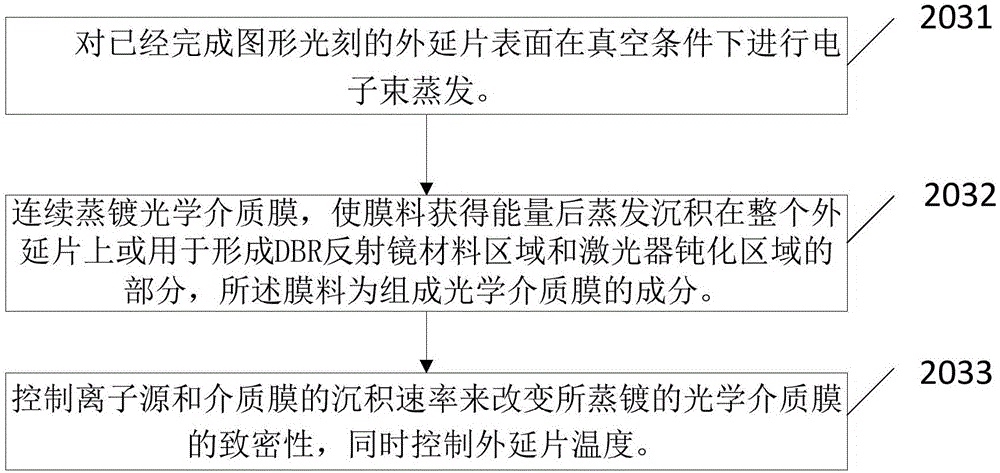
[0088] In the embodiment of the present invention, the preparation of the passivation film and the material of the DBR reflector is completed in the same vacuum chamber at one time, which not only improves the performance of the laser, but also reduces the possible damage caused by the numbe...

Embodiment 2

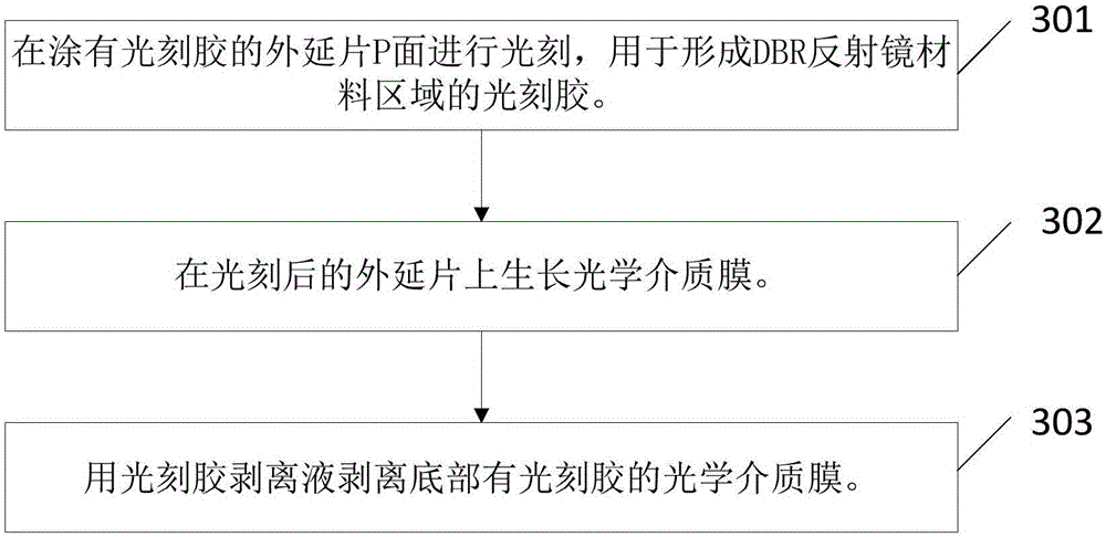
[0100] Corresponding to the preparation method of a vertical cavity surface laser based on optical dielectric film passivation described in Example 1, there is another embodiment in the present invention, a preparation of a vertical cavity surface laser based on an optical dielectric film as a DBR material method, using optical dielectric film as DBR reflector material, such as image 3 shown, including:

[0101] In step 301, photolithography is performed on the surface P of the epitaxial wafer coated with photoresist to form the photoresist in the material region of the DBR reflector.

[0102] In step 302, an optical dielectric film is grown on the epitaxial wafer after photolithography.

[0103] In step 303, the optical medium film with the photoresist at the bottom is stripped with a photoresist stripper.

[0104] The laser of the present invention adopts the optical dielectric film as the DBR mirror material, which reduces the series resistance, absorption loss and inter...

Embodiment 3

[0115] Corresponding to the preparation method of a vertical cavity surface laser based on the passivation of the optical dielectric film described in Example 1, there is also an embodiment in the present invention, wherein the laser uses the optical dielectric film as the passivation medium of the laser cavity surface film, such as Figure 5 Shown, described passivation dielectric film preparation process comprises:

[0116] In step 401, photolithography is performed on the surface P of the epitaxial wafer coated with photoresist, which is used for the photoresist in the passivation region of the laser cavity surface.

[0117] In step 402, an optical dielectric film is grown on the epitaxial wafer after photolithography.

[0118] In step 403, the optical medium film with the photoresist at the bottom is stripped with a photoresist stripper.

[0119] In a specific implementation, the step 402 can usually be implemented by the following steps, such as Image 6 Shown:

[012...


PUM


Abstract

The invention relates to the technical field of a semiconductor, and provides an optical dielectric film passivation-based vertical cavity surface laser and a preparation method therefor. The optical dielectric film is used as a DBR (distributed bragg reflector) reflective mirror material, and used as the passivation dielectric film of the cavity surface of the laser. By adopting the optical dielectric film to replace a conventional DBR reflective film, the series resistance, the absorption loss and the interface loss of the vertical cavity laser can be effectively lowered, thereby improving the thermal characteristics of the laser; the optical dielectric film is also a good electric dielectric film; and therefore, when the optical dielectric film is used for surface passivation of the laser, the process is simplified, the passivation cost is lowered, the cavity surface of the laser can be effectively protected, and the reliability of the laser is improved.

Description

【Technical field】 [0001] The invention relates to the technical field of semiconductor optoelectronics, in particular to a vertical cavity surface laser based on optical dielectric film passivation and a preparation method thereof. 【Background technique】 [0002] Vertical cavity surface lasers have the characteristics of high power, small size, low threshold current, simple modulation, and high electro-optical conversion rate. Vertical cavity surface lasers have the characteristics of large output power, small size, low threshold current, simple modulation, and high electro-optical conversion efficiency. With the advancement of national defense technology and the development of society, the application and demand of semiconductor lasers in various aspects are becoming more and more extensive and huge. Therefore, the research on the reliability and stability of vertical cavity surface lasers is becoming more and more important. Because the cavity surface of the laser is pron...

Claims


Application Information

Patent Timeline
Patent Type & Authority Applications(China)
IPC IPC(8): H01S5/183H01S5/187
CPCH01S5/18361H01S5/187
Inventor 姜勋财王任凡岳爱文汤宝罗彪吴振华余兵朱拓
Owner GUANGXUN SCI & TECH WUHAN
Why Eureka
Try Eureka