Forming method of fin type field-effect transistor

A technology of fin field effect transistors and fins, which is applied in the direction of electrical components, circuits, semiconductor devices, etc., can solve the problem of large roughness of gate sidewall line width, etc., to avoid channel length changes, high smoothness, The effect of optimizing electrical properties

Active Publication Date: 2017-01-04
SEMICON MFG INT (SHANGHAI) CORP
View PDF3 Cites 3 Cited by
  • Summary
  • Abstract
  • Description
  • Claims
  • Application Information

AI Technical Summary

Problems solved by technology

[0006] The problem to be solved by the present invention is to provide a method for forming a fin f

Method used


Image

  • Forming method of fin type field-effect transistor
  • Forming method of fin type field-effect transistor
  • Forming method of fin type field-effect transistor

Examples


Embodiment Construction

[0030] It can be seen from the background art that the electrical performance of the fin field effect transistor formed in the prior art still needs to be improved.

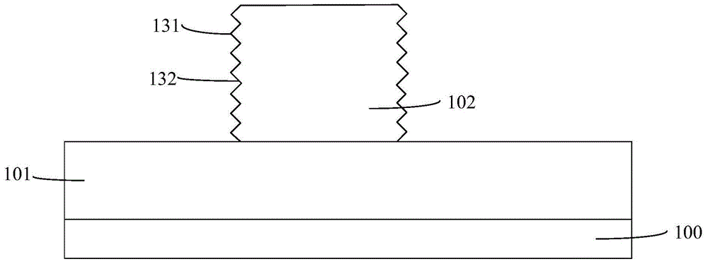
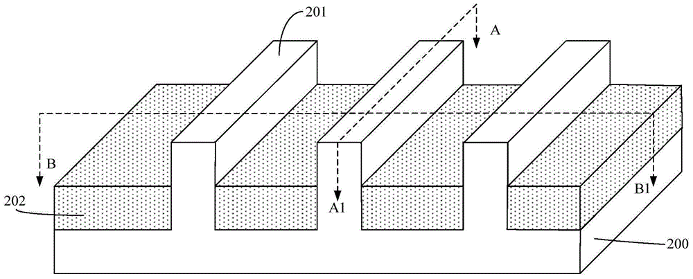
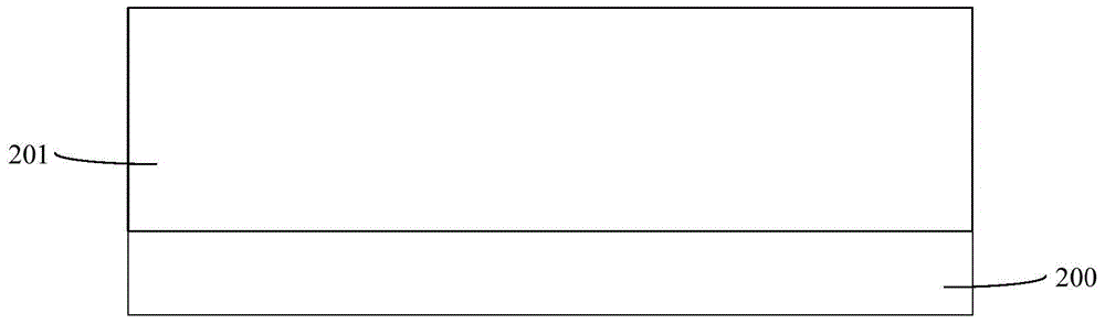
[0031] It is found through research that with the continuous reduction of the size of semiconductor structures, a new method for forming a fin field effect transistor is proposed, including: step S1, providing a substrate and several discrete fins on the surface of the substrate, the substrate A gate film is formed on the bottom surface and the surface of the fin, and the top of the gate film is higher than the top of the fin; step S2, forming several discrete first mask layers on the surface of the gate film, and the first mask The arrangement direction of the layers is consistent with the extending direction of the fins; step S3, using the first mask layer as a mask, etching the gate film until the surface of the substrate is exposed, and then removing the first mask layer; step S4 , forming several discrete se...


PUM


Abstract

A forming method of a fin type field-effect transistor comprises the steps of forming a silicon material layer on a film surface of a gate; forming a plurality of discrete first pattern layers on the silicon material layer, wherein the first pattern layers stretches across at least one fin part, and the arrangement direction of the first pattern layers is parallel to the extending direction of the fin part; taking the first pattern layers as a mask, and etching the silicon material layer until the film surface of the gate is exposed, and forming a plurality of discrete initial silicon layers on the film surface of the gate, wherein the initial silicon layers and a surface of a side wall perpendicular to the extending direction of the fin part have first line width roughness; and performing repairing etching treatment on the initial silicon layers and the side wall perpendicular to the extending direction of the fin part so that the initial silicon layers and the surface of the side wall perpendicular to the extending direction of the fin part have second line width roughness, wherein the second line width roughness is smaller than the first line width roughness. By the forming method, the quality of the formed gate is improved, the line width roughness of the gate and the side wall perpendicular to the extending direction of the fin part is improved, and thus, the electrochemical performance of the fin type field-effect transistor is improved.

Description

technical field [0001] The invention relates to the technical field of semiconductor manufacturing, in particular to a method for forming a fin field effect transistor. Background technique [0002] With the continuous development of semiconductor process technology, the development trend of semiconductor process nodes following Moore's Law continues to decrease. In order to adapt to the reduction of process nodes, the channel length of MOSFET field effect transistors has to be continuously shortened. The shortening of the channel length has the advantages of increasing the die density of the chip and increasing the switching speed of the MOSFET field effect tube. [0003] However, as the channel length of the device is shortened, the distance between the source and the drain of the device is also shortened, so that the control ability of the gate to the channel becomes worse, and the gate voltage pinches off the channel. The difficulty is also increasing, making the pheno...

Claims


Application Information

Patent Timeline
IPC IPC(8): H01L29/78H01L21/8234H01L21/302
CPCH01L21/302H01L29/66477H01L29/785
Inventor 张海洋张城龙
Owner SEMICON MFG INT (SHANGHAI) CORP
Why Eureka
Try Eureka