

Technological method of shield grid trench-type power MOS device
A technology of MOS devices and process methods, which is applied in semiconductor devices, semiconductor/solid-state device manufacturing, electrical components, etc., can solve the problems of poor withstand voltage, insufficient film thickness, and low withstand voltage of trench gates, and achieve film thickness uniformity Better, reduce the generation of easy breakdown points, and grow well
- Summary
- Abstract
- Description
- Claims
- Application Information
AI Technical Summary
Problems solved by technology
Method used
Image

Examples
Embodiment Construction
[0019] A process method of a shielded gate trench type power MOS device according to the present invention comprises the following process steps:
[0020] In the first step, trench etching is performed on the silicon substrate, and then a sacrificial oxide layer is formed; as image 3 shown.
[0021] The second step is to deposit a pad oxide layer, deposit polysilicon and etch back to form the underlying polysilicon in the trench; as Figure 4 shown.
[0022] The 3rd step, carry out polysilicon interlayer dielectric oxide film growth; Figure 5 shown.
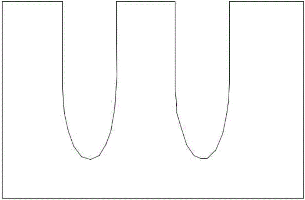
[0023] In the 4th step, a layer of thermal oxide layer is grown on the entire silicon chip surface; the thickness of the thermal oxide layer formed is like Figure 6 shown.
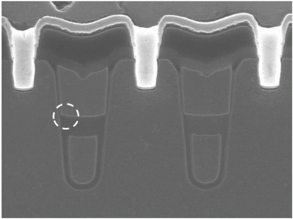
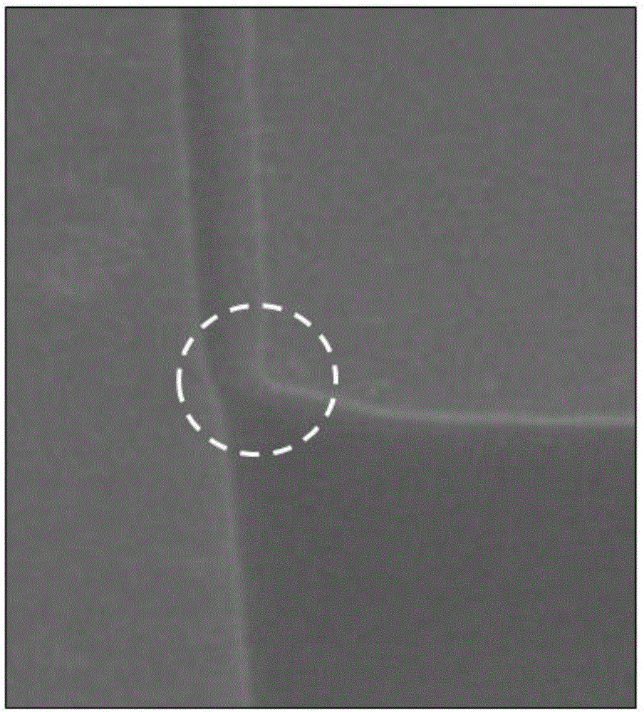
[0024] Step 5, etching back the thermal oxide layer; removing all the thermal oxide layer formed on the surface of the silicon wafer. After the thermal oxide layer process, the angle transition between the upper surface of the underlying polysilico...
PUM
 Abstract
Description
Claims
Application Information