Indium arsenide antimony and indium gallium arsenide antimony two-waveband infrared detector and manufacturing method thereof

An infrared detector, indium gallium arsenic antimony technology, applied in semiconductor devices, final product manufacturing, sustainable manufacturing/processing, etc., to achieve high quantum efficiency, improve quality, and smooth surface

Active Publication Date: 2017-01-04
INST OF SEMICONDUCTORS - CHINESE ACAD OF SCI
View PDF3 Cites 9 Cited by
  • Summary
  • Abstract
  • Description
  • Claims
  • Application Information

AI Technical Summary

Problems solved by technology

It is predicted by theoretical calculation that the performance of type II superlattice infrared detectors is the best, but there is still a gap of 1-2 orders of magnitude between the measured results and the theoretical results, indicating that the material growth and device technology need to be further improved.

Method used


Image

  • Indium arsenide antimony and indium gallium arsenide antimony two-waveband infrared detector and manufacturing method thereof
  • Indium arsenide antimony and indium gallium arsenide antimony two-waveband infrared detector and manufacturing method thereof

Examples


Embodiment Construction

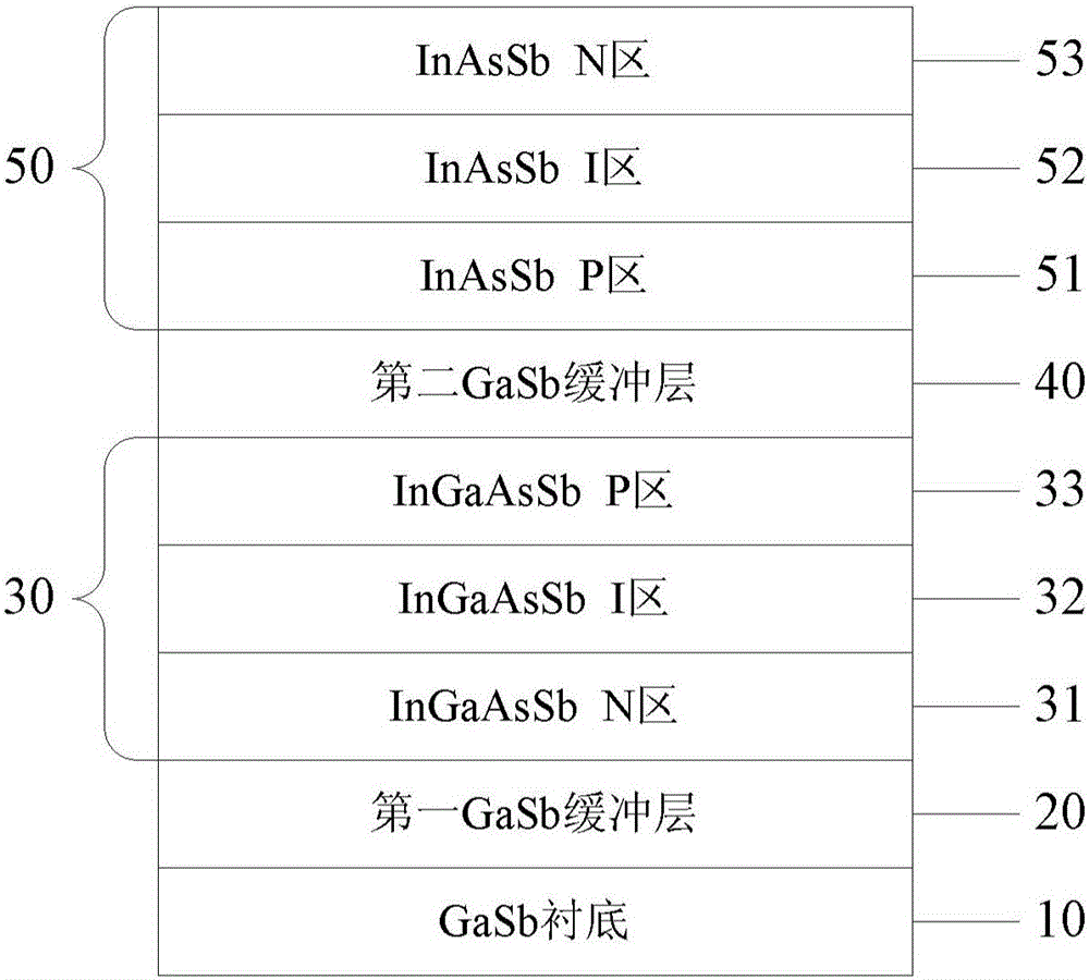
[0023] see figure 1 As shown, the indium arsenic antimony and indium gallium arsenic antimony dual-band infrared detector structure provided by the present invention includes:

[0024] a GaSb substrate 10;

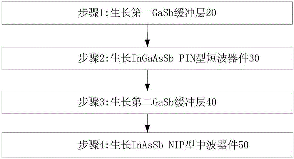
[0025] a first GaSb buffer layer 20 grown on the GaSb substrate 10;

[0026] An InGaAsSb PIN type short-wave device 30, which is grown on the first GaSb buffer layer 20. The InGaAsSb PIN type short-wave device 30 includes sequentially grown: InGaAsSb N region 31, InGaAsSb I region 32 and InGaAsSb P region 33;

[0027] A second GaSb buffer layer 40, which is grown on the InGaAsSb PIN type short-wave device 30;

[0028] An InAsSb NIP type medium wave device 50, which is grown on the second GaSb buffer layer 40. The InAsSb NIP type medium wave device 50 includes: InAsSb P region 51, InAsSb I region 52 and InAsSb N region 53 grown in sequence.

[0029] The temperature for growing the first GaSb buffer layer 20 and the second GaSb buffer layer 40 is 500°C-600°C, and the Sb / G...


PUM


Abstract

The invention provides an indium arsenide antimony and indium gallium arsenide antimony two-waveband infrared detector and a manufacturing method thereof. The indium arsenide antimony and indium gallium arsenide antimony two-waveband infrared detector structurally comprises a GaSb substrate, a first GaSb buffer layer grown on the GaSb substrate, an InGaAsSb PIN type short-wave device grown on the first GaSb buffer layer, a second GaSb buffer layer grown on the InGaAsSb PIN type short-wave device and an InAsSb NIP type middle-wave device grown on the second GaSb buffer layer. The indium arsenide antimony and indium gallium arsenide antimony two-waveband infrared detector can realize signal detection on an infrared middle-wave waveband and a short-wave waveband.

Description

technical field [0001] The invention relates to the field of molecular beam epitaxial growth of semiconductor materials, in particular to the structure of an indium arsenic antimony and indium gallium arsenic antimony dual-band infrared detector device structure and a preparation method thereof. Background technique [0002] GaSb-based semiconductor materials, including lattice constants of InAs, GaSb, AlSb and their multiple compounds, compared with the traditional mercury cadmium telluride system and quantum dot structure, have shown great potential in optics and electricity, and are popular new materials for the preparation of infrared detectors. Including InGaAsSb, InAsSb, InAs / GaSb superlattice, InAs / InAsSb superlattice and other material systems. [0003] Infrared detector is the core of infrared technology, and its development level restricts the application of infrared technology. The infrared detectors developed in the early stage have problems such as single wav...

Claims


Application Information

Patent Timeline
Patent Type & Authority Applications(China)
IPC IPC(8): H01L31/0304H01L31/18
CPCH01L31/03046Y02P70/50
Inventor 孙姚耀韩玺王国伟徐应强牛智川
Owner INST OF SEMICONDUCTORS - CHINESE ACAD OF SCI
Why Eureka
Try Eureka