Resistor loaded ultra wide band plane semi-elliptical antenna

A semi-elliptical, ultra-wideband technology, applied to antennas, devices and circuits that make the antennas work in different bands at the same time, can solve the problems of unfavorable size and system integration, difficult impedance matching, low input impedance, etc. The effect of compactness, suppression of external interference, and good broadband characteristics

Inactive Publication Date: 2017-01-04
HENAN NORMAL UNIV
View PDF7 Cites 3 Cited by
  • Summary
  • Abstract
  • Description
  • Claims
  • Application Information

AI Technical Summary

Problems solved by technology

Although the butterfly antenna has the advantages of wide frequency bandwidth, good radiation characteristics, simple fabrication, and low cost, the input impedance of the butterfly antenna designed with a rectangular shielding cavity and resistance loading is generally around 200Ω, which is not suitable for ultra-wideband antennas working in the high frequency band. The impedance matching between the butterfly antenna and the transmitter is relatively difficult, and its size is not conducive to system integration. The bandwidth and impedance conversion ratio have become the difficulties in the design of the feeding structure. Therefore, it is necessary to design a planar dipole antenna , and an antenna with a relatively low and smooth input impedance and a small lateral size is necessary

Method used


Image

  • Resistor loaded ultra wide band plane semi-elliptical antenna
  • Resistor loaded ultra wide band plane semi-elliptical antenna
  • Resistor loaded ultra wide band plane semi-elliptical antenna

Examples


Embodiment Construction

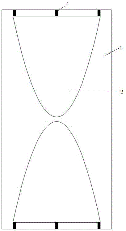
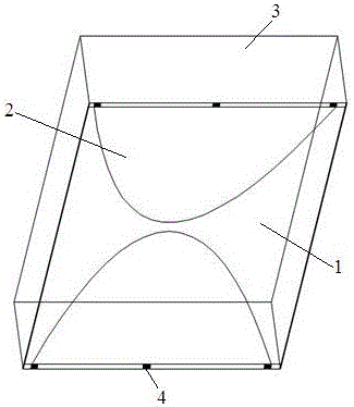
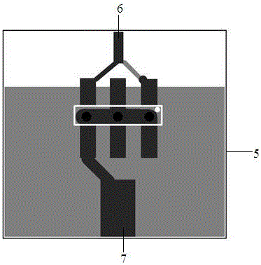
[0019] The specific content of the present invention will be described in detail in conjunction with the accompanying drawings. figure 1 It is a schematic diagram of the plane structure of a resistance-loaded ultra-wideband planar semi-elliptical antenna, such as figure 1 As shown, the resistance-loaded ultra-wideband planar semi-elliptical antenna includes an insulating dielectric plate 1, two semi-elliptical metal radiation arms 2, a metal shielding cavity 3, six loading resistors 4, absorbing materials, a feed unit and a coaxial connector , wherein the metal shielding cavity 3 is a rectangular low-reflection cavity with an open front end, which is used to shield backward radiation and suppress external interference. The insulating dielectric plate 1 is fixed at the front opening of the metal shielding cavity 3, and two semi-elliptical metal radiation arms 2 pass through The circuit board printing technology is symmetrically printed on the front of the insulating medium boar...


PUM


Abstract

The invention discloses a resistor loaded ultra wide band plane semi-elliptical antenna. A metallic shielding cavity is a rectangular low-reflection cavity with an opening in the front end; an insulated dielectric plate is fixed at the position of the opening in the front end of the metallic shielding cavity; semi-elliptical metal radiation arms are symmetrically printed on the front of the insulated dielectric plate; an interval is preset between the semi-elliptical metal radiation arms; input ports are formed in the two adjacent semi-elliptical metal radiation arms at an interval respectively as respective feed ends; loading resistors are symmetrically welded between the bottom edges of the semi-elliptical metal radiation arms and the side plate of the metallic shielding cavity; a feed unit is an FR4 dielectric plate carrying a commercial transmission line transformer; the balanced output end of the transmission line transformer is connected with the semi-elliptical metal radiation arms respectively; one end of a coaxial connector is welded with a micro-strip input end of the transmission line transformer, and the other end of the coaxial connector is connected with a transmitter and a receiver of a life detection radar system. The resistor loaded ultra wide band plane semi-elliptical antenna has good broadband characteristic and time domain radiation characteristic, and is compact in structure and simple in feeding mode.

Description

technical field [0001] The invention belongs to the technical field of ultra-wideband imaging radar antennas, in particular to a resistance-loaded ultra-wideband planar semi-elliptical antenna. Background technique [0002] In recent years, various major natural disasters and man-made accidents at home and abroad have occurred from time to time, causing a large number of casualties. Especially in densely populated cities with densely populated high-rise buildings and criss-crossing pipelines and lines, how to effectively carry out life-saving detection and positioning after disasters and improve rescue efficiency has always been a key issue. As a non-contact real-time imaging radar system, ultra-wideband radar can detect and image obstacles such as reinforced concrete brick walls, asphalt layers, debris flows and snow caused by avalanches, so it has attracted widespread attention from all walks of life. [0003] Antenna is a vital part of the radar system, its performance d...

Claims


Application Information

Patent Timeline
Patent Type & Authority Applications(China)
IPC IPC(8): H01Q1/38H01Q5/50
CPCH01Q1/38H01Q5/50
Inventor 李雪萍王立詹华伟翟炎杰施艳艳王萌
Owner HENAN NORMAL UNIV
Why Eureka
Try Eureka