Ceramic packaging device of semiconductor laser

A technology of ceramic packaging and lasers, which is applied in the direction of semiconductor lasers, lasers, laser components, etc., can solve problems such as unsatisfactory, and achieve the effects of high emission pointing accuracy, compressed device size, and good reliability

Active Publication Date: 2017-01-04
BEIJING SURESTAR TECH
View PDF6 Cites 8 Cited by
  • Summary
  • Abstract
  • Description
  • Claims
  • Application Information

AI Technical Summary

Problems solved by technology

However, in the above-mentioned prior art solutions, the size of the insulating ceramic between the base and the pins, the diameter and thickness of the base, and the height of the cap limit the reduction of the overall size of the TO package. The outer diameter of the existing TO18 package is 5.6mm, which is used in many It can no longer be used in occasions, and cannot meet the requirements of laser radar, optical fiber communication and other fields for further compression of the mechanical size and thickness of laser light sources

Method used


Image

  • Ceramic packaging device of semiconductor laser
  • Ceramic packaging device of semiconductor laser
  • Ceramic packaging device of semiconductor laser

Examples


Embodiment Construction

[0020] The technical solutions in the embodiments of the present invention will be clearly and completely described below with reference to the drawings in the embodiments of the present invention. Obviously, the described embodiments are only a part of the embodiments of the present invention, rather than all the embodiments. Based on the embodiments of the present invention, all other embodiments obtained by those of ordinary skill in the art without creative work fall within the protection scope of the present invention.

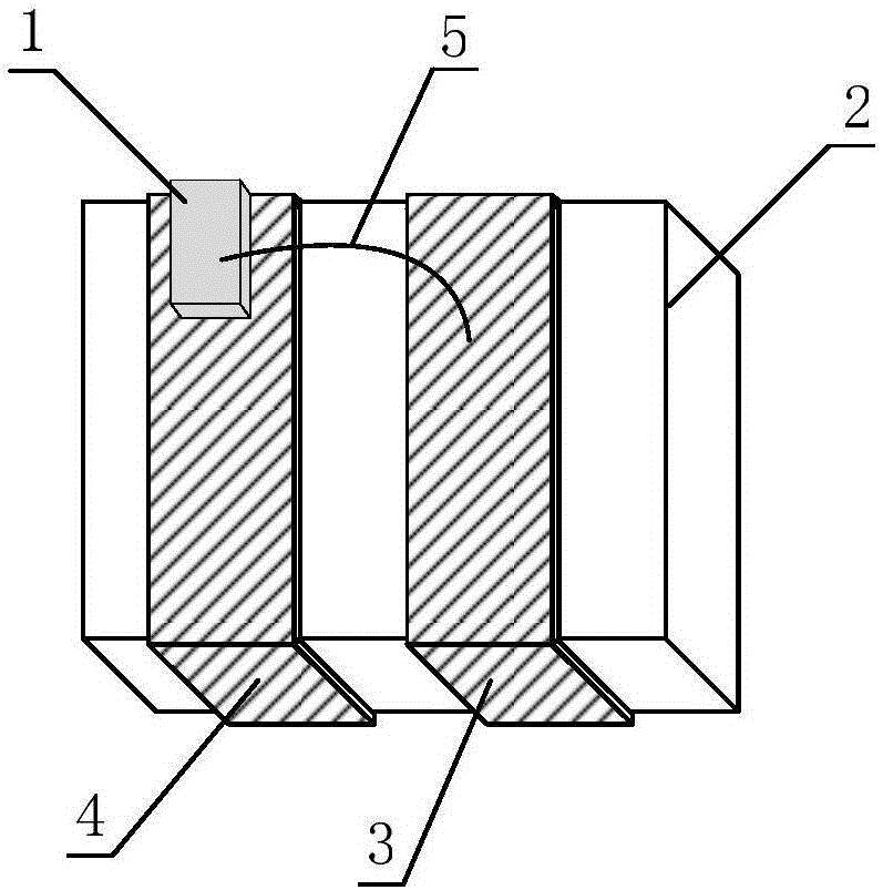
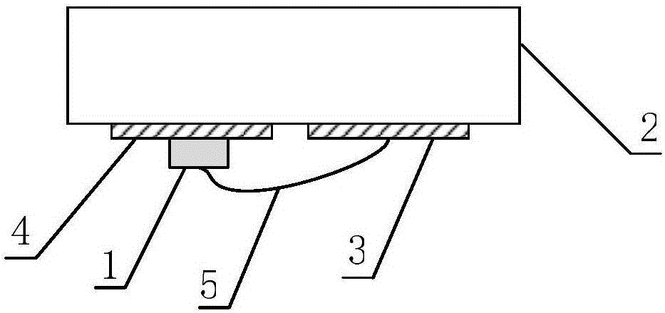
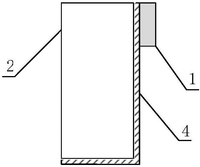
[0021] The embodiments of the present invention will be described in further detail below with reference to the accompanying drawings, such as figure 1 Shown is a schematic three-dimensional structure of a ceramic packaging device for a semiconductor laser provided by an embodiment of the present invention; as figure 2 Shown is a top view of the device provided by the embodiment of the present invention; such as image 3 Shown is a side view of the devi...


PUM


Abstract

The invention discloses a ceramic packaging device of a semiconductor laser. The device comprises an L-shaped anode soldering lug, an L-shaped cathode soldering lug and a semiconductor laser chip, wherein the L-shaped anode soldering lug is attached onto two adjacent surfaces of a heat sink carrier to form an L shape; the L-shaped cathode soldering lug and the L-shaped anode soldering lug are adjacent and parallel, and are attached onto two adjacent surfaces of the heat sink carrier to form another L shape; the semiconductor laser chip is adhered onto the top of one side of the L-shaped cathode soldering lug through a soldering material, and an anode of the semiconductor laser chip is bonded to one side of the L-shaped anode soldering lug with a soldering wire; and an anode soldering pad and a cathode soldering pad, positioned on one side of the bottom surface of the heat sink carrier, of the L-shaped anode soldering lug and the L-shaped cathode soldering lug are directly welded with a circuit board. The device is applicable to packaging of pulse type semiconductor lasers with small power, the dimensions of devices can be compressed to a greater extent, and meanwhile a more effective heat dissipation environment is provided.

Description

technical field [0001] The present invention relates to the technical field of semiconductor lasers, in particular to a ceramic packaging device for semiconductor lasers. Background technique [0002] A semiconductor laser is a laser that uses semiconductor materials such as gallium arsenide (GaAs) and indium phosphide (InP) as the working substance, and its essence is a diode chip with optical feedback capability. Semiconductor lasers have the advantages of small size, long life, and simple external drive. They are the most practical and important type of lasers, and are widely used in laser radar, laser guidance, optical fiber communication and other fields. [0003] Conventional semiconductor lasers are mostly packaged with TO (transistor outline, transistor outline), and the package form includes a TO socket, a tongue, a pin and a cap. The tube tongue is connected to the tube base, the semiconductor laser chip is glued and solidified on the tube tongue, the negative ele...

Claims


Application Information

Patent Timeline
Patent Type & Authority Applications(China)
IPC IPC(8): H01S5/024H01S5/022
CPCH01S5/022H01S5/024
Inventor 张智武
Owner BEIJING SURESTAR TECH
Why Eureka
Try Eureka