Through-silicon-via forming method and chip with through-silicon-via

A technology of through-silicon vias and chips, applied in semiconductor/solid-state device manufacturing, electrical components, circuits, etc., can solve the problems of deposition, difficult to complete film formation, and easy falling off of conductor layers.

Active Publication Date: 2017-01-11
RICHVIEW ELECTRONICS CO LTD
View PDF5 Cites 20 Cited by
  • Summary
  • Abstract
  • Description
  • Claims
  • Application Information

AI Technical Summary

Problems solved by technology

In the production process of the barrier layer/seed layer, when the existing sputtering technology manufactures through-silicon holes with small apertures and high aspect ratios, it is difficult to complete the complete film formation in the through-holes, resulting in the failure of subsequent electroplating
The aspect ratio of TSVs is usually greater than 7:1, even as high as 12:1~15:1. Conventional magnetron sputtering technology is difficult to deposit a continuous conductor layer on the sidewalls of TSVs with high aspect...

Method used


Image

  • Through-silicon-via forming method and chip with through-silicon-via
  • Through-silicon-via forming method and chip with through-silicon-via
  • Through-silicon-via forming method and chip with through-silicon-via

Examples


Embodiment Construction

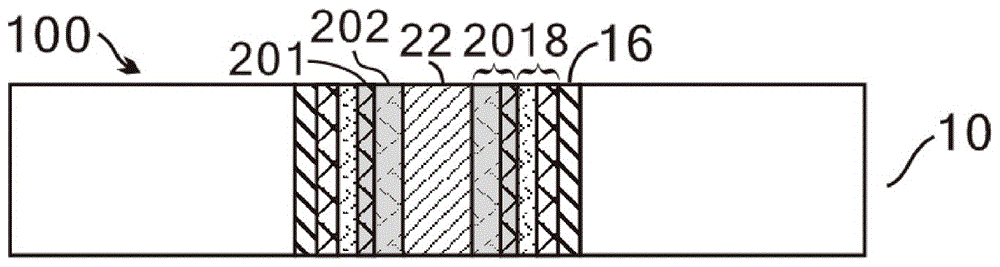
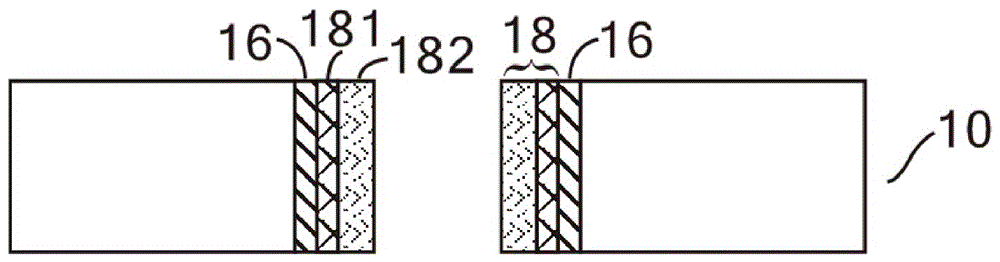
[0044] Hereinafter, embodiments of the present invention will be described in detail with reference to the accompanying drawings. It should be understood by those skilled in the art that these descriptions only illustrate exemplary embodiments of the present invention, and are not intended to limit the protection scope of the present invention. For example, elements or features described in one figure or embodiment of the invention may be combined with other elements or features described in one or more other figures or embodiments. In addition, in order to facilitate the description of the positional relationship between the various material layers, spatially relative terms are used herein, such as "upper" and "lower", and "inner" and "outer", etc., these terms are relative to the substrate. In terms of the surface or pore wall. For example, material A is considered to be above or outside material B if it is located in a direction toward the exterior of the substrate or pore...


PUM

PropertyMeasurementUnit
Thicknessaaaaaaaaaa
Thicknessaaaaaaaaaa
Thicknessaaaaaaaaaa

Abstract

The invention relates to a through-silicon-via forming method and a chip with a through-silicon-via. The through-silicon-via forming method includes the steps: S1 forming a through hole in a silicon wafer; S2 forming an insulating layer on the wall of the through hole; S3 forming a diffusion barrier layer on the insulating layer; S4 forming a seed crystal layer on the diffusion barrier layer; S5 forming a conductor layer on the seed crystal layer, wherein the step S3 includes injecting first materials into the lower portion of the surface of the insulating layer by ion injection to form a first ion injection layer, and the step S4 includes injecting second materials into the lower portion of the surface of the diffusion barrier layer by ion injection to form a second ion injection layer.

Description

technical field [0001] The present invention generally relates to a method for manufacturing a through silicon via (TSV) and a chip including the through silicon via, which can be widely used in the interconnection between chips and the packaging technology of stacked chips In order to form a 3D packaging structure. Background technique [0002] In recent years, computers, communications, automotive electronics, aerospace industry and other consumer products have put forward high requirements for microelectronic packaging, that is, smaller, thinner, lighter, high reliability, multi-function, low power consumption and low cost. This has prompted the emergence of higher-density three-dimensional stacked packaging technologies. Three-dimensional stacked packaging can be divided into stacking of packages and stacking of silicon wafers. Currently, the stacking technology of packages can be obtained by stacking thin small outline packages (TSOPs) or stacking chip-scale packages...

Claims


Application Information

Patent Timeline
IPC IPC(8): H01L21/768H01L21/265
CPCH01L21/265H01L21/76822
Inventor 宋红林王志健杨志刚张志强
Owner RICHVIEW ELECTRONICS CO LTD
Why Eureka
Try Eureka