
Process method for adding ILD (Inter Layer Deposition) filling window of adjustable control gate poly

A process method and control gate technology, which are applied to electrical components, electrical solid-state devices, circuits, etc., can solve the problems of increasing the aspect ratio of the unit storage area, difficulty in completely filling the trenches of the unit storage area, and affecting the reliability and performance of the device. , to reduce the aspect ratio, improve the flatness, and the process is simple and controllable.

Active Publication Date: 2017-01-11
SHANGHAI HUALI MICROELECTRONICS CORP
View PDF3 Cites 3 Cited by
  • Summary
  • Abstract
  • Description
  • Claims
  • Application Information

AI Technical Summary

Problems solved by technology

[0011] At present, the peripheral device area and the control gate of the unit storage area of ​​the floating gate nonvolatile memory can be deposited in one step by furnace tube technology, and the thickness is generally about 2000 angstroms, while the unit storage area of ​​the floating gate nonvolatile memory device In addition to the control gate with the same thickness as the peripheral device area, there is also a floating gate structure with a thickness of about 1000 angstroms. As the size of NVM continues to decrease, the aspect ratio of the space trench in the cell storage area increases greatly. , in the ILD (interlayer Deposition) process, it is very easy to generate voids (void), and it becomes very difficult to completely fill the trenches in the cell storage area, which will seriously affect the reliability of the device

Method used


Image

  • Process method for adding ILD (Inter Layer Deposition) filling window of adjustable control gate poly
  • Process method for adding ILD (Inter Layer Deposition) filling window of adjustable control gate poly
  • Process method for adding ILD (Inter Layer Deposition) filling window of adjustable control gate poly

Examples


Embodiment Construction

[0049] Embodiments embodying the features and advantages of the present invention will be described in detail in the following description. It should be understood that the invention can have various changes in different examples without departing from the scope of the invention, and that the descriptions and illustrations therein are illustrative in nature rather than limiting the invention.

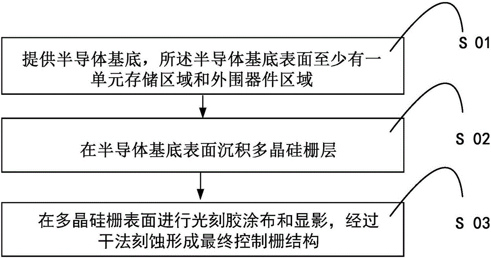
[0050] The process method of increasing the ILD filling window with the adjustable control gate of the present invention will be further described in detail with reference to the accompanying drawings. It should be noted that the problem solved by the present invention is to reduce the thickness of the control gate in the storage area of ​​the unit while maintaining the thicker polysilicon gate layer in the peripheral device area.

[0051] Specific embodiments of the present invention will be described in detail below in conjunction with the accompanying drawings.

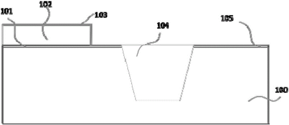
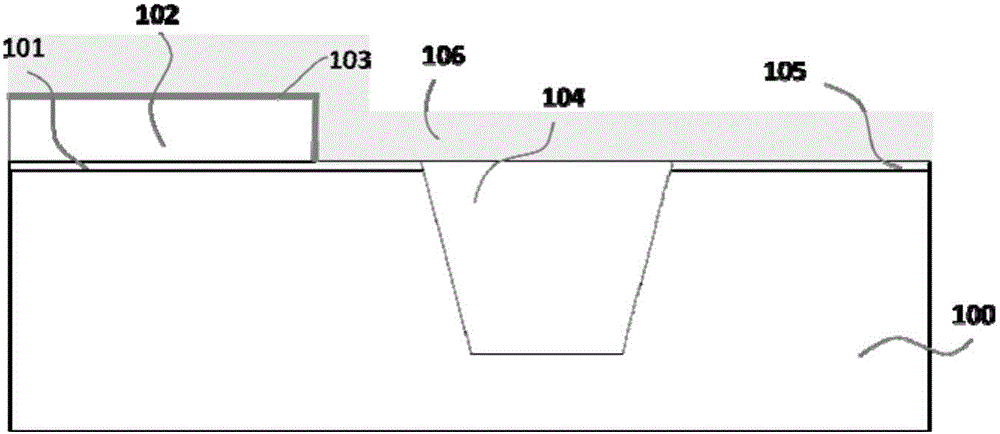
[0052] see Figure...


PUM


Abstract

A process method for adding an ILD (Inter Layer Deposition) filling window of an adjustable control gate poly comprises the steps of providing a substrate with a cell memory region and a peripheral region; depositing a first poly gate layer on a surface of the substrate; growing a silicon oxide blocking layer on a surface of the first poly gate layer; performing photoresist coating and developing on a surface of the silicon oxide blocking layer to expose the peripheral region, and only etching to remove the silicon oxide blocking layer on the peripheral region; depositing second poly gate layers on surfaces of the silicon oxide blocking layer of the cell memory region and the first poly gate layer of the peripheral region; performing photoresist coating and developing on a surface of the second poly gate layers to expose the cell memory region, and etching to only remove the second poly gate layer on the cell memory region; etching to remove the remaining silicon oxide blocking layer; and performing photoresist coating and developing on surfaces of poly gates of the cell memory region and the peripheral region, and forming a final dual-poly gate structure by dry etching.

Description

technical field [0001] The invention relates to the field of integrated circuit manufacturing, in particular to a process method for increasing an ILD filling window with an adjustable control gate. Background technique [0002] A floating gate type non-volatile memory (Non-volatile memory, referred to as NVM) is a common integrated circuit device, which includes a source, a drain, a gate and a floating gate (Floating Gate). Generally, a floating-gate nonvolatile memory structure can be formed using a classic stack-gate process. The polysilicon layer close to the tunnel oxide layer is used as a floating gate, the top polysilicon layer is used as a control gate poly, and the insulating layer between the two polysilicon layers is a silicon dioxide or ONO (Oxide-Nitride-Oxide) structure. The effect of isolating the floating gate area. [0003] Compared with volatile memory, due to the existence of floating gate, non-volatile memory can still maintain data information even whe...

Claims


Application Information

Patent Timeline
Patent Type & Authority Applications(China)
IPC IPC(8): H01L27/11517H10B41/00
CPCH10B41/00
Inventor 刘政红辻直樹陈广龙
Owner SHANGHAI HUALI MICROELECTRONICS CORP
Features
  • Generate Ideas
  • Intellectual Property
  • Life Sciences
  • Materials
  • Tech Scout
  • Unparalleled Data Quality
  • Higher Quality Content
  • 60% Fewer Hallucinations
Learn More