Carrier storage type grooved-gate IGBT (insulated gate bipolar transistor)

A carrier storage and trench gate technology, applied in electrical components, circuits, semiconductor devices, etc., can solve the problems of insignificant improvement in device performance and reduced device withstand voltage, so as to improve the withstand voltage capability and improve the trade-off relationship. Effect

Inactive Publication Date: 2017-01-25
UNIV OF ELECTRONIC SCI & TECH OF CHINA
View PDF3 Cites 6 Cited by
  • Summary
  • Abstract
  • Description
  • Claims
  • Application Information

AI Technical Summary

Problems solved by technology

However, the lower concentration of the charge storage layer has no obvious effect on the improvement of the device performance, so in order to better improve the performance of the devi

Method used


Image

  • Carrier storage type grooved-gate IGBT (insulated gate bipolar transistor)
  • Carrier storage type grooved-gate IGBT (insulated gate bipolar transistor)
  • Carrier storage type grooved-gate IGBT (insulated gate bipolar transistor)

Examples


Embodiment 1

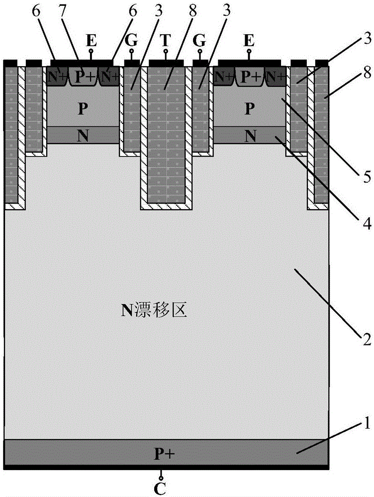
[0025] Such as figure 1 As shown, this example includes a P+ collector region 1, an N drift region 2, a groove gate structure 3 and an emitter active region, and the groove gate structure 3 and the emitter active region are alternately arranged on the surface of the N drift region (2) , the emitter active region is sequentially composed of an N storage layer 4, a P-type body region 5, and an emitter doped region from bottom to top, the bottom of the N storage layer 4 is higher than the bottom of the trench gate structure 3, and the emitter The doped region is composed of N+ regions 6 on both sides and a P+ region 7 between the two N+ regions 6. It is characterized in that it also includes a deep groove structure 8, which is composed of the medium of the groove wall and the P+ region 7. The conductive material surrounded by it, the deep groove structure 8 runs through the entire groove gate structure 3 from the surface of the groove gate structure 3 and goes deep into the insid...

Embodiment 2

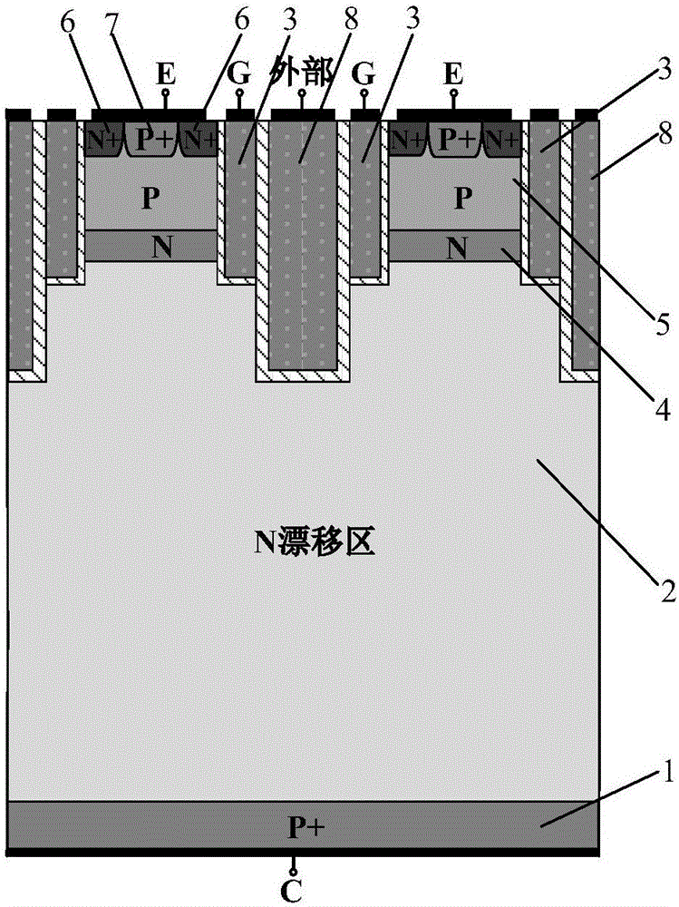
[0029] Such as figure 2 As shown, the basic structure of this embodiment is the same as that of Embodiment 1, except that the deep groove structure 8 is connected to the emitter electrode through a conductive material instead of being connected to an external variable electrode.

[0030] This example works as follows:

[0031] When the device is in forward conduction, the deep groove structure 8 at low potential can accumulate a layer of holes on the surface to enhance the conductance modulation effect, thereby further reducing the conduction voltage drop. In addition, since the deep groove structure is connected to the emitter, there is basically no influence on the "gate-collector" capacitance (that is, "Miller capacitance") of the device; The beneficial effects are the same.

[0032] As a simple modification of this embodiment, the deep trench structure 8 can also be connected to the gate electrode through a conductive material, which can also improve the withstand volta...

Embodiment 3

[0034] Such as image 3 As shown, the basic structure of this embodiment is the same as that of Embodiment 1, except that there is an N-type buffer layer 9 above the P+ collector region 1 , and the concentration of this buffer layer is higher than that of the N-type drift region 2 .

[0035] In addition to the beneficial effects described in Embodiment 1, this example has a punch-through withstand voltage structure due to the existence of the N-type buffer layer 9, which can make the device have a shorter drift region length under the same withstand voltage capability. , reduces the resistance of the drift region in the on-state of the device, and can also control the hole injection efficiency of the P+ collector 1 in the forward conduction, thereby further reducing the on-state voltage drop and off-state loss.


PUM


Abstract

The invention belongs to the technical field of semiconductors and relates to a carrier storage type grooved-gate IGBT (insulated gate bipolar transistor). The carrier storage type IGBT is structurally provided with two split gates and a deep groove; when a device is in a closed state, a carrier storage layer of the device is exhausted by adopting assistance of a deep groove, and meanwhile, the deep grove and the split gates form a stepped structure to weaken the peak value of an electric field of an emitter, so that voltage endurance capability of the device under higher carrier storage layer concentration is obviously improved. In addition, when the device is in an open state, a layer of the carriers can be further accumulated on the surface of a deep-groove structure 8, and conduction pressure of the device is further reduced.

Description

technical field [0001] The invention belongs to the technical field of semiconductors, and in particular relates to a carrier storage type IGBT (Insulated Gate Bipolar Transistor, insulated gate bipolar transistor). Background technique [0002] Energy consumption is increasing day by day, especially the demand contradiction of electric power is becoming more and more acute. It has become an important subject to vigorously develop new power electronic devices. IGBT is currently the fastest growing hybrid power electronic device. It has the characteristics of MOS input, bipolar output function, MOS and bipolar combination. It has high input impedance of MOSFET, small control power, simple driving circuit, The advantages of high switching speed and low switching loss, as well as the advantages of high current density, low saturation voltage, and strong current handling capability of bipolar power transistors, are unmatched by other power devices in terms of high voltage, high ...

Claims


Application Information

Patent Timeline
IPC IPC(8): H01L29/06H01L29/739
CPCH01L29/7397H01L29/0623H01L29/7398
Inventor 罗小蓉阮新亮吴俊峰周坤邓高强孙涛
Owner UNIV OF ELECTRONIC SCI & TECH OF CHINA
Why Eureka
Try Eureka