Green brazing method of solar cell si chip al back electrode and cu electrode lead wire

A solar cell, electrode lead technology, applied in circuits, welding equipment, photovoltaic power generation, etc., can solve the problems of producing toxic and harmful gases and smoke, strong flux, corrosiveness, etc., to improve photovoltaic characteristics and avoid corrosive flux. Residual and cost reduction effect

Active Publication Date: 2019-03-29
HARBIN INST OF TECH
View PDF11 Cites 0 Cited by
  • Summary
  • Abstract
  • Description
  • Claims
  • Application Information

AI Technical Summary

Problems solved by technology

[0010] CN104952508A discloses a method for directly brazing an Al back electrode using a reactive flux. In the flux used, heavy metal chloride is used as a reactant, NaF and / or KF are used as a reaction aid, and NH 4 Cl and / or NH 4 Br is used as a wetting aid, but this flux has the following problems: 1) This flux is a corrosive flux, and its flux residue is highly corrosive to the joint; 2) It will produce toxic and harmful Gas and smoke; 3) Flux has a high melting point and can only be used with a small amount of Sn-based solder

Method used


Image

  • Green brazing method of solar cell si chip al back electrode and cu electrode lead wire
  • Green brazing method of solar cell si chip al back electrode and cu electrode lead wire
  • Green brazing method of solar cell si chip al back electrode and cu electrode lead wire

Examples


specific Embodiment approach 1

[0044] Embodiment 1: In this embodiment, pure Sn solder is used. The solder is wire-shaped with a diameter of 1 mm. The solar cell used is a polysilicon solar cell with a thickness of 180 μm and an Al back field thickness of 30 μm.

[0045] In the present embodiment, the method of using pure Sn solder to directly braze solar cell Al back field electrodes and Cu electrode leads is carried out according to the following steps:

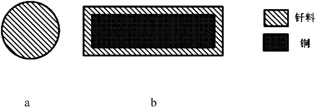
[0046] Step 1. Use an ultrasonic soldering iron to heat up to the brazing temperature. The heating temperature is 260°C. Fill the solder with solder wire. The state diagram of the solder is as follows figure 1 shown

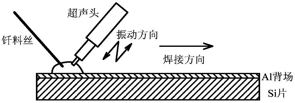
[0047] Step 2. Insert the ultrasonic tool head into the liquid solder, apply ultrasonic waves for 1 second, the frequency of the ultrasonic is 60KHz, and the amplitude range is 1μm, to remove the oxide film on the surface of Al and make the solder fully wet and spread. The brazing schematic diagram is as follows image 3 shown. In order to ...

specific Embodiment approach 2

[0050] Embodiment 2: In this embodiment, SnAgCu solder is used. The solder is in the shape of a wire with a diameter of 0.8mm, and its specific composition is Sn-3.0Ag-0.5Cu (wt.%).

[0051] In the present embodiment, the method of using SnAgCu solder to directly braze the solar cell Al back field and the Cu electrode lead is carried out according to the following steps:

[0052] Step 1. Use an ultrasonic soldering iron to heat up to the brazing temperature. The heating temperature is 240°C. Fill the solder with solder wire. The state diagram of the solder is as follows figure 1 shown.

[0053] Step 2. Insert the ultrasonic tool head into the liquid solder, apply 3s of ultrasound, the frequency of the ultrasound is 20KHz, and the amplitude range is 3μm, to remove the oxide film on the Al surface and make the solder fully wet and spread. The brazing schematic diagram is as follows image 3 shown. In order to reduce the stress level of the joint, discontinuous two strips of so...

specific Embodiment approach 3

[0055] Embodiment 3: In this embodiment, a brazing strip coated with SnBi solder is used.

[0056] In the present embodiment, the method of using the brazing strip coated with SnBi solder to directly solder the Al back field electrode of the solar cell is carried out according to the following steps:

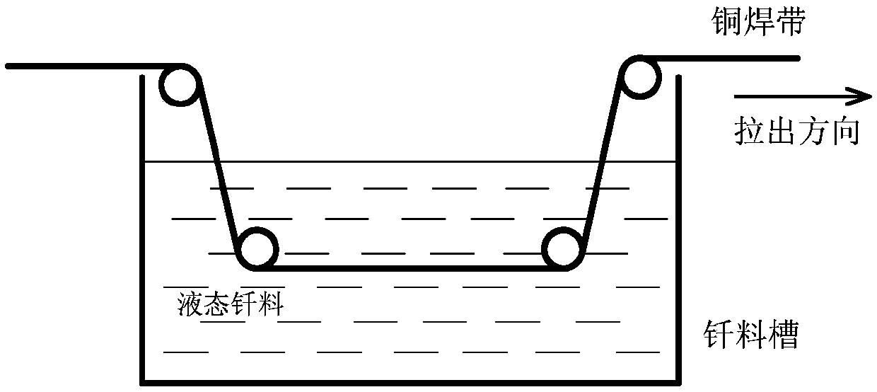
[0057] Step 1, placing Sn-58Bi (wt.%) solder in a solder tank, heating and melting, passing the copper strip continuously through the molten solder to complete the coating of the solder on the surface of the copper strip. The width of the welding strip is 2mm, the thickness of the copper strip is 0.15mm, and the thickness of the coated solder is 0.05mm. The schematic diagram of the state of the solder is shown in figure 1 As shown, the schematic diagram of brazing strip surface coated with solder is as follows figure 2 shown.

[0058] Step 2: Place the two welding strips on the Al back field, and perform infrared heating on the parts to be welded at a heating temperature of ...


PUM

PropertyMeasurementUnit
thicknessaaaaaaaaaa
thicknessaaaaaaaaaa
diameteraaaaaaaaaa

Abstract

The invention discloses an environment-friendly brazing method for the Al back electrode and Cu electrode leads of the Si wafer of a solar cell. The method includes: using lead-free Sn-based solder wires to fill solder, applying ultrasonic after the solder melts, and coating the Al back surface field of the solar cell with the solder; placing a copper solder strip on the pre-coated solder, and heating with soldering iron to melt the solder so as to form connection; or placing the copper solder strip coated with the lead-free Sn-based solder on the Al back surface field of the solar cell, and heating a to-be-welded part; applying ultrasonic after the solder melts to complete welding. The environment-friendly brazing method has the advantages that the problems that the Al back surface field electrode of the Si solar cell wafer cannot be brazed directly, brazing can only be performed after Ag welding spots are printed, and manufacturing cost increasing and performance lowering are caused are solved, the corrosion problem caused by the fact that the Al back electrode and Cu electrode leads are brazed by using brazing flux is solved, and the problem of high Si wafer damage rate caused by ultrasonic metal welding is solved.

Description

technical field [0001] The invention belongs to the field of welding technology, and relates to a welding method of a solar battery panel, in particular to a method for environmentally friendly brazing of an Al back electrode of a solar battery Si sheet and a lead wire of a Cu electrode. Background technique [0002] As a clean and renewable energy source, solar energy has already occupied an important position in the energy field. Solar photovoltaic power generation technology has also been applied and promoted worldwide, and low manufacturing cost and high performance output have become the development trend of solar panels. [0003] The output voltage and power of a single solar cell are very limited, so multiple solar cells need to be connected in series and parallel to achieve a certain power output. This requires the positive and negative electrodes of the solar cell to be welded together step by step. Silver grid wires are generally printed on the light-receiving su...

Claims


Application Information

Patent Timeline
Patent Type & Authority Patents(China)
IPC IPC(8): H01L31/18B23K1/06
CPCB23K1/06H01L31/188Y02E10/50Y02P70/50
Inventor 闫久春郭卫兵于汉臣
Owner HARBIN INST OF TECH
Why Eureka
Try Eureka