Check patentability & draft patents in minutes with Patsnap Eureka AI!

Ceramic capacitor of crystal boundary layer and manufacturing process of capacitor

A technology of ceramic capacitors and manufacturing processes, which is applied in the direction of laminated capacitors, capacitors, fixed capacitors, etc., and can solve the problems of small size of single-layer chip ceramic capacitors, lower product qualification rate and reliability, gold layer adhesion and performance decline and other problems, to achieve the effect of avoiding the decrease of adhesion, high reliability and reducing process steps

Active Publication Date: 2017-02-01
CHINA ZHENHUA GRP YUNKE ELECTRONICS
View PDF3 Cites 5 Cited by
  • Summary
  • Abstract
  • Description
  • Claims
  • Application Information

AI Technical Summary

Problems solved by technology

[0002] Single-layer chip ceramic capacitors have the characteristics of small size, many types, and high application frequency. They are widely used in electronic countermeasures, radar, navigation, guidance, and satellite communications. The market demand for this product has shown explosive growth in recent years. This product The development direction is small volume, large capacity, high voltage; grain boundary layer ceramics are favored by the industry because of their large dielectric constant (greater than 10000) and good temperature characteristics (±25%), and are widely used in single-layer Chip ceramic capacitors; however, at present, the grain boundary layer ceramics have large dielectric constant dispersion due to the special material preparation process, and the product qualification rate is very low; Fixed by the photolithography mask, the etching process is likely to cause the adhesion and performance of the gold layer to decline. This method reduces the pass rate and reliability of the product

Method used


Image

  • Ceramic capacitor of crystal boundary layer and manufacturing process of capacitor
  • Ceramic capacitor of crystal boundary layer and manufacturing process of capacitor
  • Ceramic capacitor of crystal boundary layer and manufacturing process of capacitor

Examples


Embodiment Construction

[0029] The present invention will be further explained below in conjunction with the accompanying drawings and specific embodiments.

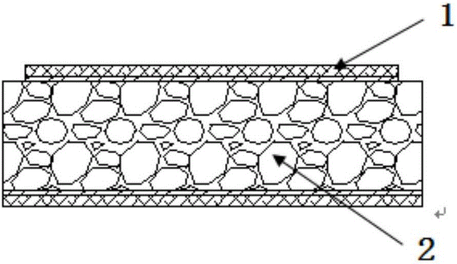
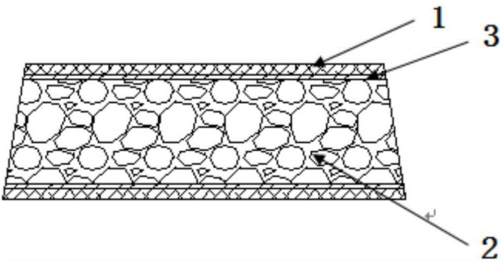
[0030] Such as figure 2 As shown, a grain boundary layer ceramic capacitor includes a gold electrode 1, a grain boundary layer ceramic 2 and a Tiw transition layer 3, and the two sides of the grain boundary layer ceramic 2 are respectively provided with a Tiw transition layer 3, and the Tiw transition layer 3 A gold electrode 1 is provided on both sides, and the gold electrode 1, the Tiw transition layer 3 and the grain boundary layer ceramic 2 have the same length. The upper and lower surfaces of the grain boundary layer capacitor are parallel, the edges are sloped, and the cross section is trapezoidal.

[0031] Single-layer chip ceramic capacitors are prepared by using a special cutting process, which greatly improves the pass rate and reliability of the product. The steps are as follows:

[0032] Step 1, check the appearance and size of th...


PUM


Abstract

The invention discloses a ceramic capacitor of a crystal boundary layer and a manufacturing process of the capacitor. The ceramic capacitor of the crystal boundary layer comprises a metal electrode, ceramics of the crystal boundary layer and a TiW transition layer. A ceramic medium of the crystal boundary layer is used, a specially cutting technology is used, and the capacitor is made in a trapezoidal structure; the capacitor is small in size and large in electric capacity; the reliability is high, processes during protection are reduced, a photoetching process is avoided, and the metal electrode is prevented from loss of adhesion; and a special scribing technology can be used to improve the qualified rate greatly and reduce the production cost.

Description

technical field [0001] The invention belongs to the technical field of grain boundary layer ceramic capacitor and its manufacturing process Background technique [0002] Single-layer chip ceramic capacitors have the characteristics of small size, many types, and high application frequency. They are widely used in electronic countermeasures, radar, navigation, guidance, and satellite communications. The market demand for this product has shown explosive growth in recent years. This product The development direction is small volume, large capacity, high voltage; grain boundary layer ceramics are favored by the industry because of their large dielectric constant (greater than 10000) and good temperature characteristics (±25%), and are widely used in single-layer Chip ceramic capacitors; however, at present, the grain boundary layer ceramics have large dielectric constant dispersion due to the special material preparation process, and the product qualification rate is very low; ...

Claims


Application Information

Patent Timeline
Patent Type & Authority Applications(China)
IPC IPC(8): H01G4/30H01G4/12H01G4/00
CPCH01G4/00H01G4/12H01G4/1281H01G4/306
Inventor 刘剑林韩玉成朱威禹黄伟训廖东
Owner CHINA ZHENHUA GRP YUNKE ELECTRONICS
Features
  • R&D
  • Intellectual Property
  • Life Sciences
  • Materials
  • Tech Scout
  • Unparalleled Data Quality
  • Higher Quality Content
  • 60% Fewer Hallucinations
Learn More