Manufacturing method of thin film chip and thin film chip thereof

A thin-film chip and manufacturing method technology, which is applied in semiconductor/solid-state device manufacturing, electrical components, circuits, etc., can solve the problems of high AlGaN layer stress, precise control of grinding, and difficulty

Active Publication Date: 2017-02-01
XIAMEN SANAN OPTOELECTRONICS TECH CO LTD
View PDF3 Cites 7 Cited by
  • Summary
  • Abstract
  • Description
  • Claims
  • Application Information

AI Technical Summary

Problems solved by technology

However, the laser lift-off method will damage the epitaxy at local high temperature and reduce the reliability of the device.
There are also methods of grinding or dry etching to remove the substrate, but the cost is high, and the grinding position and dry etching position cannot be precisely controlled
In addition, due to the lattice mismatch between GaN and AlN, at present, deep ultraviolet light-emitting diodes usually grow AlN layers on sapphire substrates, but the substrates are difficult to lift off by laser; Instantly releases stress and breaks easily
For LED chips with a flip-chip structure, the roughening effect of the sapphire substrate is poor. To roughen the back of the AlN layer, the sapphire often needs to be ground off. At present, it is difficult to achieve precise control of grinding the sapphire without grinding off the epitaxial layer.

Method used


Image

  • Manufacturing method of thin film chip and thin film chip thereof
  • Manufacturing method of thin film chip and thin film chip thereof
  • Manufacturing method of thin film chip and thin film chip thereof

Examples


Embodiment

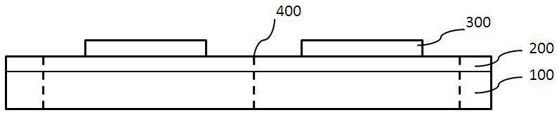
[0029] like figure 1 As shown, a light-emitting epitaxial wafer is provided. First, sapphire is used as a growth substrate 100, and an N-type III-V thin film, a light-emitting active layer, and a P-type III-V thin film are grown on the growth substrate 100, as Light emitting epitaxial stack 200 . The Group III-V thin film can be composed of boron, aluminum, gallium, indium of group III and nitrogen, phosphorus and arsenic of group V. The luminescent wavelength of the luminescent active layer is between 200-1150nm, preferably in the ultraviolet band, such as UV-C band (200-280nm), UV-B band (280-315nm) and UV-A band (315-380nm). Next, several chip structure layers 300 are fabricated on the light-emitting epitaxial stack, and dicing lines 400 are defined on the surface of the light-emitting epitaxial stack between adjacent chip structure layers, wherein the chip structure layer 300 may further include a contact layer and a mirror reflector. layer (Mirror).
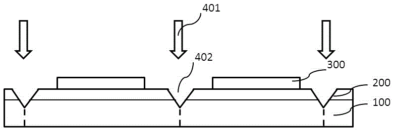
[0030] like fi...


PUM


Abstract

The invention provides a manufacturing method of a thin film chip and the thin film chip thereof. The manufacturing method comprises the following steps: providing a luminescent epitaxial wafer composed of a growth substrate and a luminescent epitaxial laminating layer, and manufacturing a plurality of chip structure layers on the luminescent epitaxial laminating layer, wherein cutting channels are defined on the surface of the luminescent epitaxial laminating layer between the adjacent chip structures; marking off groove structures on the cutting channels in advance, and running through the groove structures to the interior of the growth substrate; thinning according to the dimensions of the groove structures along the back face of the growth substrate until the growth substrate is removed and the luminescent epitaxial laminating layer is exposed out; carrying out simplified treatment, and separating the luminescent epitaxial wafer into a plurality of thin film chips.

Description

technical field [0001] The invention relates to a manufacturing method of a semiconductor light emitting device, more specifically to a manufacturing method of a thin film chip and the thin film chip. Background technique [0002] The light-emitting diode (LED) of the solid-state light-emitting device has low energy consumption, long life, good stability, small size, fast response speed and stable light-emitting wavelength and other good photoelectric characteristics, and is widely used in lighting, home appliances, display screens and indicator lights, etc. field. This type of light-emitting device has made considerable progress in terms of light efficiency and service life, and is expected to become the mainstream of a new generation of lighting and light-emitting devices. [0003] For LED chips using insulating substrates such as sapphire and AlN, the thermal conductivity of the substrate is relatively low, so the temperature of the PN junction of LEDs with a lateral str...

Claims


Application Information

Patent Timeline
Patent Type & Authority Applications(China)
IPC IPC(8): H01L33/00H01L21/78
CPCH01L21/78H01L33/0093H01L33/0095
Inventor 钟志白杨力勋李佳恩郑锦坚徐宸科康俊勇
Owner XIAMEN SANAN OPTOELECTRONICS TECH CO LTD
Why Eureka
Try Eureka