Double-frequency array antenna used for 5G (the fifth generation) wireless communication
An array antenna and wireless communication technology, applied in antenna arrays, specific array feeding systems, antennas, etc., can solve the problems of not being able to meet the 5G millimeter wave frequency band, and achieve the effects of good directivity, large bandwidth, and high radiation efficiency
- Summary
- Abstract
- Description
- Claims
- Application Information
AI Technical Summary
Problems solved by technology
Method used
Image
Examples
Embodiment 1
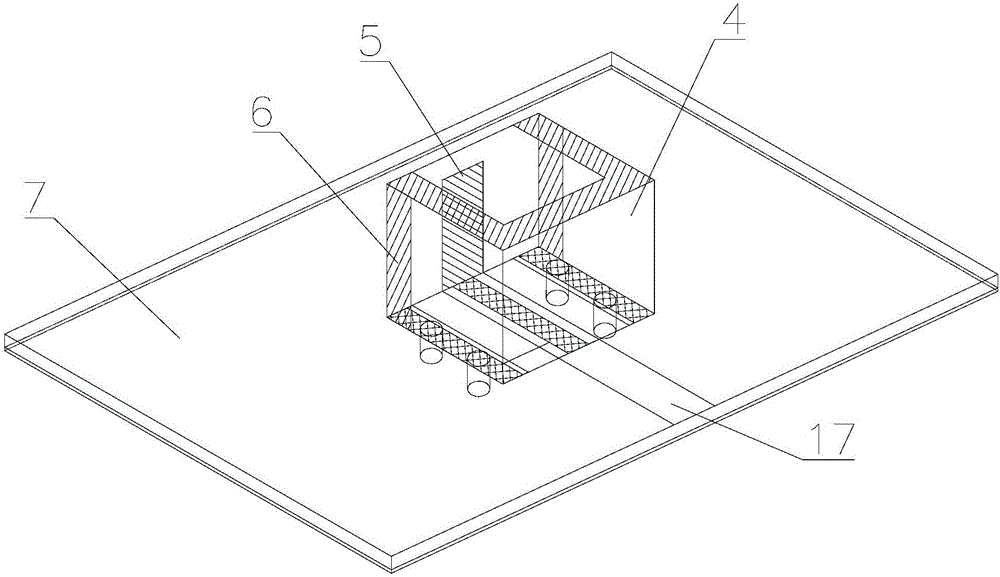
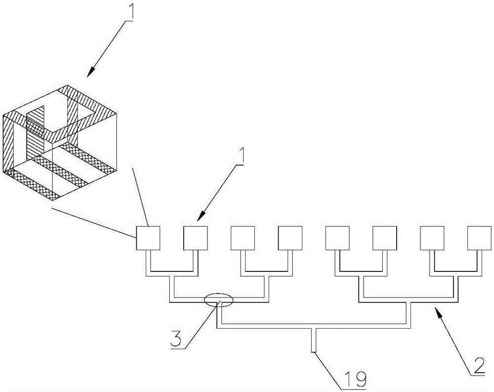
[0052] Please refer to figure 1 , image 3 and Figure 5 , this embodiment provides a dual-frequency array antenna for fifth-generation wireless communication, which can simultaneously include large bandwidths of two frequency bands of 37GHz and 39GHz, and has the advantages of high gain and radiation efficiency and good directivity, and can be used for mobile The equipment provides a millimeter-wave antenna array system for future 5G communications.
[0053] The dual-frequency array antenna includes a plurality of antenna elements 1 and a feed network 2 , and the antenna elements 1 are connected to the feed network 2 . Each antenna unit 1 includes a three-dimensional antenna carrier 4 and a PCB board 7; the surface of the three-dimensional antenna carrier 4 is surrounded by a first antenna radiator 5 and a second antenna radiator 6, which generate different resonance points respectively to realize dual frequency characteristics. Each resonance point is generated by differ...
Embodiment 2
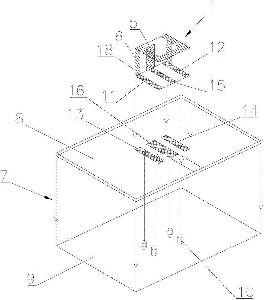
[0062] Please refer to figure 2 , this embodiment further expands the structure of the dual-frequency antenna unit on the basis of the first embodiment.
[0063] Specifically, the bottom surface of the three-dimensional antenna carrier 4 of the antenna unit 1 is respectively provided with a first pad 11 and a second pad 12 corresponding to two ends of the second antenna radiator 6 . The PCB board 7 includes a PCB substrate 8 and a PCB floor 9; the upper surface (PCB substrate 8) of the PCB board 7 is respectively provided with a third pad 13 corresponding to the first pad 11 and the second pad 12 and the fourth pad 14, which are connected to the PCB floor 9 through the via hole 10; the two ends of the second antenna radiator 6 are respectively connected to the first pad 11 and the second pad 12, and the first pad The pad 11 and the second pad 12 are correspondingly connected to the third pad 13 and the fourth pad 14 .
[0064] The solid connection between the three-dimensio...
Embodiment 3
[0069] In this embodiment, on the basis of the first and second embodiments, the structure of the dual-frequency antenna unit is further expanded.
[0070] Specifically, the three-dimensional antenna carrier 4 can be a rectangular three-dimensional structure (a cube structure or a cuboid structure), or a columnar three-dimensional structure such as a cylinder; its material can be ceramics or other materials with good permittivity. In this embodiment, the three-dimensional antenna carrier 4 is a rectangular three-dimensional ceramic.
[0071] Since the size of the antenna radiator is determined by the permittivity ε of the antenna carrier r It is determined that the larger the dielectric constant of the carrier, the shorter the wavelength. In this embodiment, due to the use of permittivity ε r =8.0 ceramic material, its dielectric constant is relatively large, so the size of the antenna radiator can be reduced, the size of the antenna monomer will also be reduced, and the ove...
PUM
| Property | Measurement | Unit |
|---|---|---|
| Return loss | aaaaa | aaaaa |
Abstract
Description
Claims
Application Information


