LED upside-down mounting structure

A LED chip, flip chip technology, applied in electrical components, electrical solid devices, circuits, etc., can solve the problems of large device size, low light output, and refraction.

Active Publication Date: 2017-02-08
GUANGDONG UNIV OF TECH
View PDF4 Cites 5 Cited by
  • Summary
  • Abstract
  • Description
  • Claims
  • Application Information

AI Technical Summary

Problems solved by technology

like Image 6 Shown is a packaging method in the prior art. In this packaging method, the flip chip is first bonded to the substrate, and then the fluorescent plastic mold is pushed onto the substrate to form a five-sided package for the LED chip, and finally on the fluorescent glue. Then coat the packaging adhesive layer to complete the mold top packaging of components, but this packaging method has low light output, unsatisfactory heat dissipation, and relatively large device size
[0003] In addition, in some existing flip-chip structures, the reflective layer is usually made of transparent plastic. In the process of product miniaturization and thinning of the reflective layer, the light emitted by the LED chip can easily pass through the reflective layer. It will cause insufficient light saturation of the product, and also cause halo phenomenon in the packaging structure due to the refraction of light passing through the reflective layer, which further affects the luminous efficiency of the LED, and will also lead to a decrease in color rendering index and color loss. Coordinate offset and other issues

Method used


Image

  • LED upside-down mounting structure
  • LED upside-down mounting structure
  • LED upside-down mounting structure

Examples


Embodiment 1

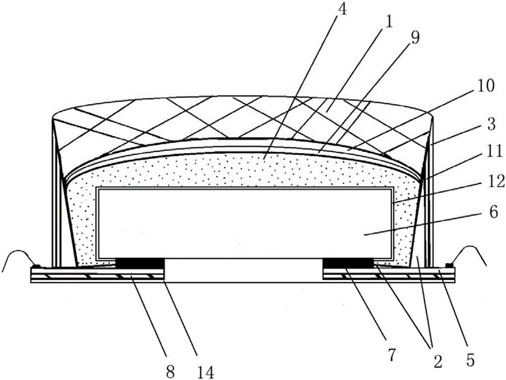
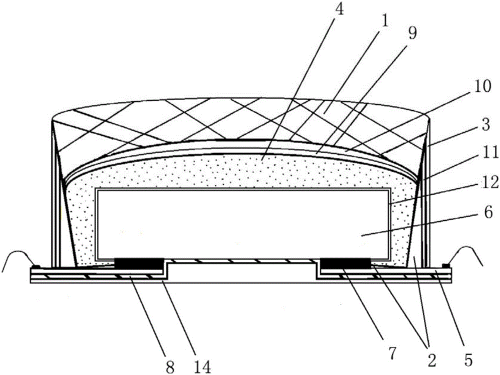
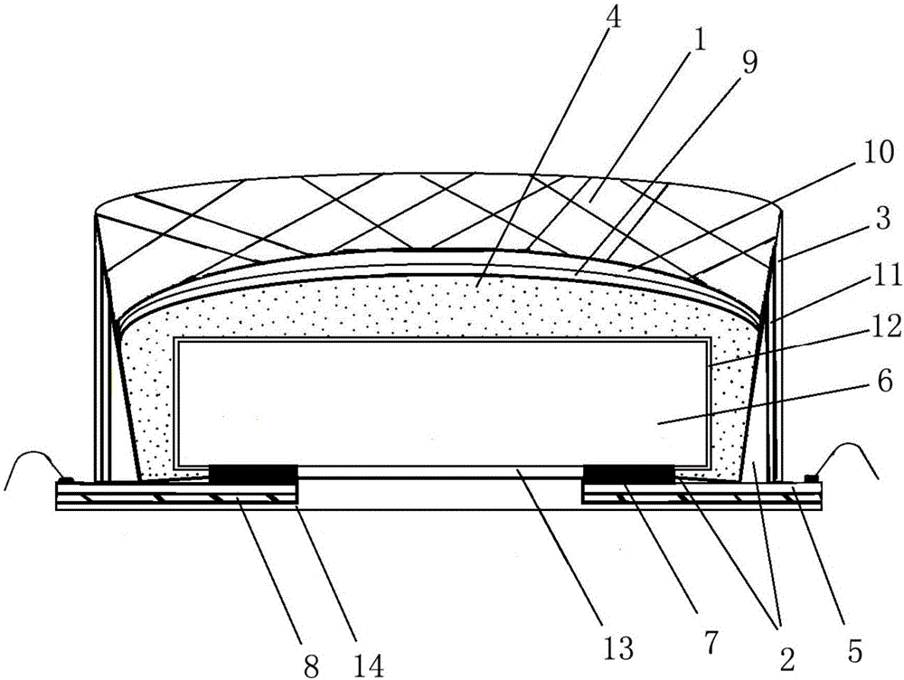
[0045] Such as figure 1 As shown, the present invention discloses an LED flip-chip structure, which mainly includes an LED chip 6, an insulating reflective cup 2, a fluorescent glue 4, a packaging glue layer 1, a conductive film 5, a welding pad 7, and a lens 9, which are used to improve the light extraction rate. An anti-reflection film 10 for reducing reflection effect, a silicon rubber layer 12 , and a sapphire substrate 14 . The conductive films 5 and the pads 7 are separated and insulated from each other. The insulating reflective cup 2 is arranged on the conductive film 5 and fixedly connected with the conductive film 5 for reflecting the light emitted by the LED chip 6 and fixing the packaging form of the LED. The bottom of the conductive film 5 is also provided with a ceramic film 8 for heat dissipation, and the ceramic film 8 of the sapphire substrate protrudes upwards between the two conductive films 5 to form a boss for isolating the conductive film 5, increasing ...

Embodiment 2

[0066] Such as figure 1 As shown, an LED flip-chip structure includes: LED chip 6, lens 9 doped or coated with fluorescent powder, fluorescent glue 4, insulating reflective cup 2, metal reflective cup 11, anti-reflection film 10, packaging adhesive layer 1. Transparent silicone rubber layer 12, welding pad 7, high temperature resistant conductive film 5, light absorbing layer 3, ceramic film 8 of sapphire substrate, thermal conductive adhesive layer 13. The LED chip 6 adopting the flip-chip structure is encapsulated in the fluorescent glue 4, and the surface of the LED chip is coated with a transparent silicone layer 12 with a high refractive index. The high-temperature conductive film 5 is electrically connected, and the upper surface of the fluorescent glue 4 is equipped with a lens 9 that is internally mixed or coated with phosphor powder. The upper surface of the lens 9 is also provided with an anti-reflection film 10 that enhances light transmission. 10 The upper surfac...


PUM


Abstract

The invention discloses an LED upside-down mounting structure. Silica gel is uniformly plated on an LED chip. Fluorescent glue is plated on the surface of silica gel. The upper surface of the fluorescent glue is provided with a lens. The upper surface of the lens is provided with an anti-reflection film. The upper surface of the anti-reflection film is provided with a packaging glue layer. The silica gel and the fluorescent glue are successively filled in an insulated reflection cup. A metal reflection cup is arranged outside the insulated reflection cup. A light absorbing layer is arranged outside the metal reflection cup. The packaging glue layer is filled among the reflection cup, the lens and the light absorbing layer. A sapphire substrate on a lowest layer is preprocessed for forming an inverse-T-shaped structure. One ceramic film epitaxial wafer is grown on the surface of the inverse-T-shaped structure. Then a high-temperature-resistant conductive film is grown on the upper surface of grooves at two ends. A heat conductive glue layer with certain thickness is uniformly plated on the boss of the inverse-T-shaped structure. The LED upside-down mounting structure can prevent a halo effect. Furthermore the LED upside-down mounting structure has advantages of effective light outlet quality improvement, excellent heat radiation performance, small packaging dimension and easier optical matching.

Description

technical field [0001] The invention relates to the technical field of LED semiconductor packaging, in particular to an LED packaging structure with high light extraction rate and good heat dissipation. Background technique [0002] The LED industry has attracted much attention in recent years. LED products have the advantages of energy saving, environmental protection, power saving, high efficiency, fast response, long service life, and mercury-free. In order to obtain the required brightness and color for LED high-power products, a layer of potting compound with high refractive index is coated on the surface of the LED chip, and a reflective layer is set in the LED packaging structure. With the increasing maturity of flip-chip technology, there are various packages for flip-chip structures. Such as Figure 6 Shown is a packaging method in the prior art. In this packaging method, the flip chip is first bonded to the substrate, and then the fluorescent plastic mold is pushe...

Claims


Application Information

Patent Timeline
Patent Type & Authority Applications(China)
IPC IPC(8): H01L33/48H01L33/64H01L33/58H01L33/60H01L33/56H01L33/54H01L33/62
CPCH01L33/486H01L33/54H01L33/56H01L33/58H01L33/60H01L33/62H01L33/641H01L33/44H01L33/64H01L2224/04H01L2924/18161
Inventor 何苗杨思攀熊德平周俊楠
Owner GUANGDONG UNIV OF TECH
Why Eureka
Try Eureka