MOS pipe and preparation method thereof

A technology for MOS tubes and metal grids, which is applied in the field of MOS tubes and its preparation, can solve the problems of high requirements on gate morphology and photoresist exposure morphology, increased production costs, and difficult implementation, so as to shorten production time, suppress leakage current, and achieve the effect of low difficulty

Inactive Publication Date: 2017-02-15
TRULY HUIZHOU SMART DISPLAY
View PDF6 Cites 3 Cited by
  • Summary
  • Abstract
  • Description
  • Claims
  • Application Information

AI Technical Summary

Problems solved by technology

Among them, the method of adding a mask increases the production cost, and the method of lightly doping the drain without

Method used


Image

  • MOS pipe and preparation method thereof
  • MOS pipe and preparation method thereof
  • MOS pipe and preparation method thereof

Examples


Embodiment Construction

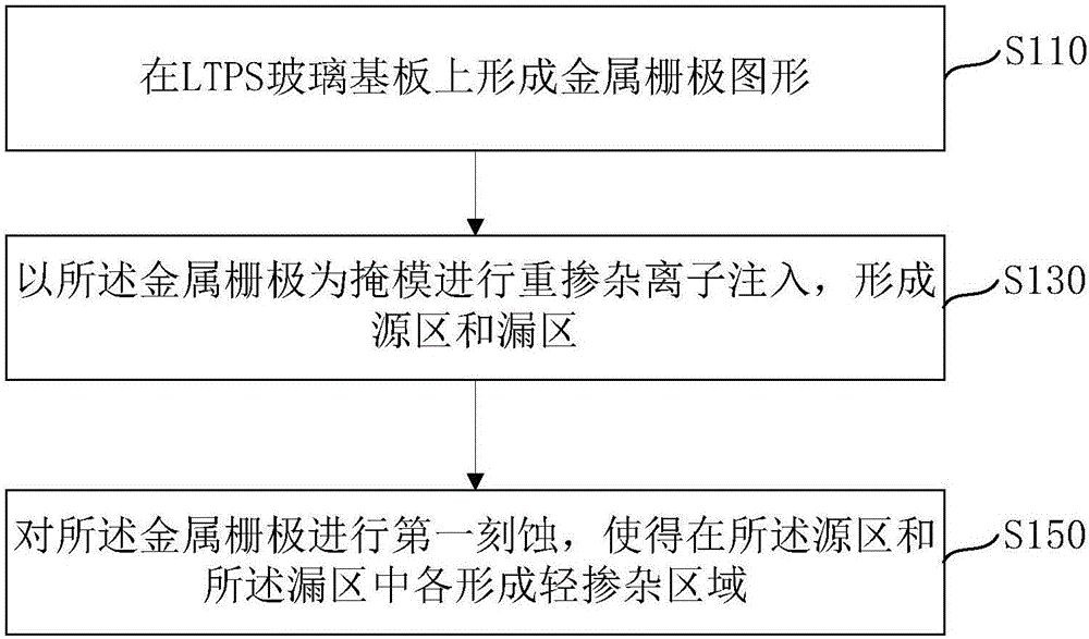
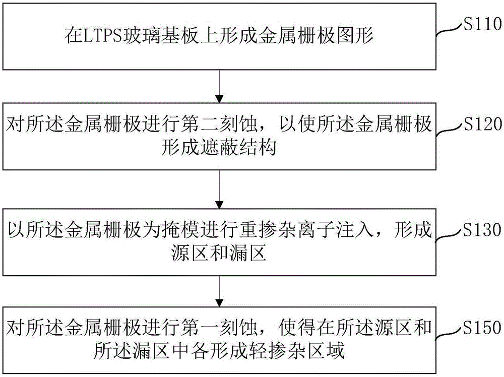
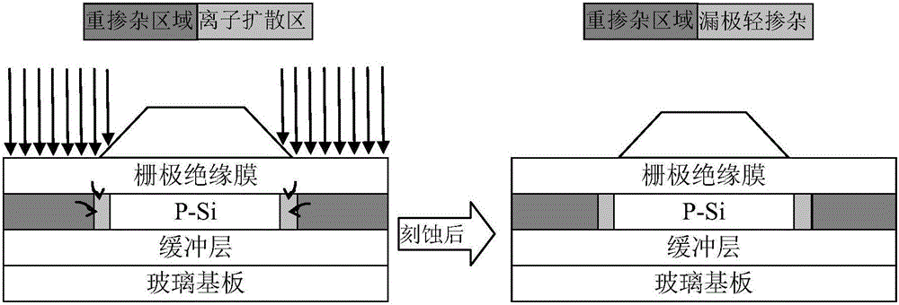
[0036] In order to make the object, technical solution and advantages of the present invention clearer, the present invention will be further described in detail below in conjunction with the accompanying drawings and embodiments. It should be understood that the specific embodiments described here are only used to explain the present invention, not to limit the present invention.

[0037] In the description of the present invention, it should be understood that the terms "first" and "second" are used for description purposes only, and cannot be interpreted as indicating or implying relative importance or implicitly indicating the quantity of indicated technical features. Thus, the features defined as "first" and "second" may explicitly or implicitly include at least one of these features. In the description of the present invention, "plurality" means at least two, such as two, three, etc., unless otherwise specifically defined.

[0038] The MOS tube and its manufacturing met...


PUM

PropertyMeasurementUnit
Thicknessaaaaaaaaaa

Abstract

The present invention provides a MOS pipe and a preparation method thereof. The preparation method comprises: forming a metal grid figure on a LTPS (Low Temperature Poly-silicon) glass substrate; taking the metal grid as a mask to perform high doping ion implantation, and forming a source region and a drain region; and performing first etching of the metal grid to form lighting doping regions in the source region and the drain region. The preparation method of the MOS pipe, after the high doping ion implantation is performed, a technology of etching the metal grid is added to automatically form light doping regions in the source region and the drain region so as to effectively inhibit leakage current, further reduce the contact barriers of the metal and the semiconductor to some extent, and reduce the contact resistances of the source metal, the drain metal and the polycrystalline silicon. The MOS pipe and the preparation method thereof can effectively inhibit the leakage current with no need for increasing extra mark plates and reduce the realization difficulty so as to reduce the production cost and shorten the production time.

Description

technical field [0001] The invention relates to the field of display technology, in particular to a MOS tube and a preparation method thereof. Background technique [0002] LTPS (Low Temperature Poly-silicon, low-temperature polysilicon) technology is a technology that projects laser light on a glass substrate with an amorphous silicon structure, so that the glass substrate with an amorphous silicon structure absorbs laser energy and transforms it into a polysilicon structure. Since liquid crystal displays using LTPS substrates have the advantages of high resolution, high brightness, high aperture ratio, and fast response speed, LTPS technology is currently widely used in display technology. [0003] In practical applications, the performance of LTPS is worse than that of crystalline silicon, especially when forming a PMOS device, there is a disadvantage of large leakage current. In order to reduce the leakage current, a method of lightly doping the drain is generally used ...

Claims


Application Information

Patent Timeline
IPC IPC(8): H01L21/336H01L29/786
CPCH01L29/78675H01L29/66757
Inventor 张豪峰张帆陈建荣任思雨苏君海李建华
Owner TRULY HUIZHOU SMART DISPLAY
Why Eureka
Try Eureka