
Laser

A technology of lasers and laser pulses, applied in the field of lasers, can solve problems such as low efficiency, appearance quality and electrical yield decline, and achieve the effects of reducing costs, improving appearance effects, and improving quality

Inactive Publication Date: 2017-02-15
GAUSS LASERS TECH (SHANGHAI) CO LTD
View PDF17 Cites 10 Cited by
  • Summary
  • Abstract
  • Description
  • Claims
  • Application Information

AI Technical Summary

Problems solved by technology

[0007] In view of the above-mentioned shortcomings of the prior art, the object of the present invention is to provide a laser for solving the problems of low scribing efficiency of laser slicing for thicker wafers, reduced appearance quality and electrical yield in the prior art

Method used


Image

  • Laser
  • Laser
  • Laser

Examples


Embodiment Construction

[0035] The following describes the implementation of the present invention through specific specific examples, and those skilled in the art can easily understand other advantages and effects of the present invention from the content disclosed in this specification. The present invention can also be implemented or applied through other different specific embodiments, and various details in this specification can also be modified or changed based on different viewpoints and applications without departing from the spirit of the present invention.

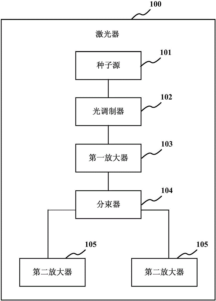
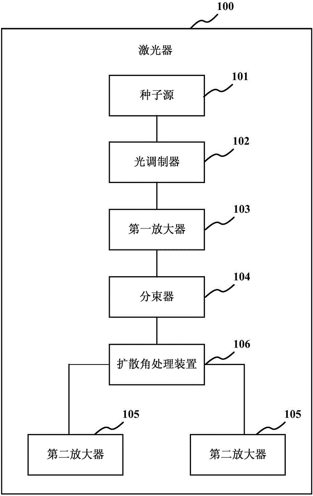
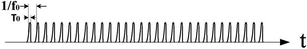
[0036] The purpose of this embodiment is to provide a laser that uses a pulse train of femtosecond or picosecond laser beams for dicing substrates such as LED chip substrates.

[0037] The laser of this embodiment is a common source dual optical path pulse train picosecond fiber laser, which is generated from the same picosecond seed source, two paths, with adjustable envelope, composed of 2 or more ultrashort laser pulses Pulse train (2-2 ...


PUM


Abstract

The invention provides a laser comprising a seed source, an optical modulator, a first amplifier, a beam splitter, and two second amplifiers. The seed source is used for outputting a laser pulse with an adjustable frequency and an adjustable pulse width. The optical modulator is used for modulating the laser pulse to an optical pulse string having a certain envelope shape under control of a modulation signal. The first amplifier is used for amplifying the optical pulse to improving the laser power of the optical pulse string. The beam splitter is used for dividing the amplified optical pulse string into a first pulse string and a second pulse string identical with the first pulse string. The two second amplifiers are used for amplifying the first pulse string and the second pulse string respectively to improve the laser powers of the first pulse string and the second pulse string. According to the laser, with focusing, two pulses are processed into a cutting layer that have an upper layer and a lower layer that are formed by a plurality of focusing points being explosion points respectively on a to-be-scribed object. The laser is suitable for one-time cutting of a thick LED wafer; the appearance linearity and appearance effect of thick wafer processing are improved; and the laser scribing quality is enhanced effectively.

Description

Technical field [0001] The present invention relates to the technical field of laser processing applications, in particular to a laser. Background technique [0002] Laser cutting is a new cutting technology developed compared to the traditional saw blade cutting in the industry. It generally focuses the laser beam on the surface or inside of the chip, uses the laser to make groove marks on the surface or inside of the chip, and then uses the split technology Split along the scratch. Laser cutting has the advantages of high productivity, high yield, easy automated operation, low cost, etc. It is widely used in the preparation of LED (light emitting diode) chips, RFID (radio frequency identification), Flash (flash memory) and other products, especially in In the substrate dicing process of semiconductor LED chips, diamond cutter cutting has been completely replaced. [0003] The use of laser processing technology for LED wafer dicing has become a standard process in the LED manufa...

Claims


Application Information

Patent Timeline
Patent Type & Authority Applications(China)
IPC IPC(8): H01S3/00H01S3/10H01L33/00H01L21/67
CPCH01S3/0007H01L21/67011H01L33/005H01S3/10
Inventor 周士安任红艳吴明
Owner GAUSS LASERS TECH (SHANGHAI) CO LTD
Features
  • Generate Ideas
  • Intellectual Property
  • Life Sciences
  • Materials
  • Tech Scout
  • Unparalleled Data Quality
  • Higher Quality Content
  • 60% Fewer Hallucinations
Learn More