Visible broad-spectrum depolarizing beam splitter

A depolarized spectroscopic and wide-spectrum technology, which is applied in the field of spectroscopic sheets, can solve the problems of complex processing technology, low final yield, and high processing cost, and achieve the effects of simple physical structure and optical structure, reduced processing cost, and reduced processing difficulty

Active Publication Date: 2017-02-22
FOCTEK PHOTONICS LNC
View PDF6 Cites 0 Cited by
  • Summary
  • Abstract
  • Description
  • Claims
  • Application Information

AI Technical Summary

Problems solved by technology

It is realized by coating the slope of the prism and gluing the paired prisms. The processing technology is complicated, the processing process is long, the final yield is low, and the processing cost is high.

Method used


Image

  • Visible broad-spectrum depolarizing beam splitter
  • Visible broad-spectrum depolarizing beam splitter
  • Visible broad-spectrum depolarizing beam splitter

Examples


Embodiment 1

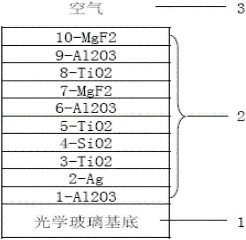
[0026] A visible wide-spectrum depolarization spectroscopic sheet, the spectroscopic sheet is composed of an optical glass substrate and a spectroscopic film deposited on the optical glass substrate, the spectroscopic film is composed of 10 film layers, and the thickness of the 10 film layers is sequentially : Layer 1, dielectric material Al 2 o 3 The thickness of the film layer is 4.99nm; the second layer, the metal material Ag film layer, the thickness is 25.6nm; the third layer, the dielectric material TiO 2 Film layer with a thickness of 32.9nm; the fourth layer, dielectric material SiO 2 Film layer with a thickness of 140.1nm; the fifth layer, dielectric material TiO 2 Film layer with a thickness of 25.2nm; the sixth layer, dielectric material Al 2 o 3 The thickness of the film layer is 110.5nm; the seventh layer, the dielectric material MgF2 film layer, the thickness is 130.7nm; the eighth layer, the dielectric material TiO 2 Film layer with a thickness of 13.4nm; t...

Embodiment 2

[0030] A visible wide-spectrum depolarization spectroscopic sheet, the spectroscopic sheet is composed of an optical glass substrate and a spectroscopic film deposited on the optical glass substrate, the spectroscopic film is composed of 10 film layers, and the thickness of the 10 film layers is sequentially : Layer 1, dielectric material Al 2 o 3 The thickness of the film layer is 5.0nm; the second layer, the metal material Ag film layer, the thickness is 25.3nm; the third layer, the dielectric material TiO 2Film layer with a thickness of 32.5nm; the fourth layer, dielectric material SiO 2 Film layer with a thickness of 138.7nm; the fifth layer, dielectric material TiO 2 Film layer with a thickness of 25.0nm; the sixth layer, dielectric material Al 2 o 3 The thickness of the film layer is 109.4nm; the seventh layer, the dielectric material MgF2 film layer, the thickness is 129.4nm; the eighth layer, the dielectric material TiO 2 Film layer with a thickness of 13.3nm; the...

Embodiment 3

[0034] A visible wide-spectrum depolarization spectroscopic sheet, the spectroscopic sheet is composed of an optical glass substrate and a spectroscopic film deposited on the optical glass substrate, the spectroscopic film is composed of 10 film layers, and the thickness of the 10 film layers is sequentially : Layer 1, dielectric material Al 2 o 3 The thickness of the film layer is 5.1nm; the second layer, the metal material Ag film layer, the thickness is 25.8nm; the third layer, the dielectric material TiO 2 Film layer with a thickness of 33.2nm; the fourth layer, dielectric material SiO 2 Film layer with a thickness of 141.5nm; the fifth layer, dielectric material TiO 2 Film layer with a thickness of 25.5nm; the sixth layer, dielectric material Al 2 o 3 The thickness of the film layer is 111.6nm; the seventh layer, the dielectric material MgF2 film layer, the thickness is 132.0nm; the eighth layer, the dielectric material TiO 2 Film layer with a thickness of 13.6nm; th...


PUM


Abstract

The invention relates to a visible broad-spectrum depolarizing beam splitter. The beam splitter consists of an optical glass substrate and a beam splitting film, wherein the beam splitting film consists of the following 10 film layers sequentially from inside to outside: a 1st layer: a dielectric material Al2O3 film layer; a 2nd layer: a metal material Ag film layer; a 3rd layer: a dielectric material TiO2 film layer; a 4th layer: a dielectric material SiO2 film layer; a 5th layer: a dielectric material TiO2 film layer; a 6th layer: a dielectric material Al2O3 film layer; a 7th layer: a dielectric material MgF2 film layer; an 8th layer: a dielectric material TiO2 film layer; a 9th layer: a dielectric material Al2O3 film layer; and a 10th layer: a dielectric material MgF2 film layer. Through the beam splitter, the processing difficulty is effectively reduced, the processing cost is lowered, and the design production is facilitated; and moreover, the film layers are of good hardness and firmness, the working band is 450-650nm, the permeation-reflection ratio is 45:45, and the difference between component S and component P is less than +/-5%.

Description

technical field [0001] The invention relates to a spectroscopic sheet, in particular to a visible wide-spectrum depolarization spectroscopic sheet. Background technique [0002] Beam splitters are widely used in optoelectronic instruments, laser systems, photoelectric display systems, and optical storage. Usually, beam splitters are used at an angle to split the incident light into reflected light and transmitted light. When the light is obliquely incident on the optical film, since the tangential components of the electric field and magnetic field are continuous on each interface, the effective refractive index of the S component and the P component will be different, which makes the film inevitably produce a polarization effect. People often This characteristic is used to design and manufacture optical polarization devices such as polarization beam splitters. However, in other optical system applications, it is desirable to eliminate polarization effects. [0003] The de...

Claims


Application Information

Patent Timeline
Patent Type & Authority Applications(China)
IPC IPC(8): G02B5/30
CPCG02B5/3041
Inventor 朱元强
Owner FOCTEK PHOTONICS LNC
Why Eureka
Try Eureka