
Structure for reducing noise in cmos image sensors

A technology of image sensors and field effect transistors, applied in the direction of semiconductor devices, electric solid state devices, diodes, etc., can solve the problems of inconvenience and lack of structure of general products, achieve accuracy and quality improvement, improve cost structure, and easily achieve with the effect obtained

Active Publication Date: 2006-09-13
TAIWAN SEMICON MFG CO LTD
View PDF0 Cites 1 Cited by
  • Summary
  • Abstract
  • Description
  • Claims
  • Application Information

AI Technical Summary

Problems solved by technology

[0005] It can be seen that the above-mentioned existing image sensor obviously still has inconvenience and defects in structure and use, and needs to be further improved urgently.
In order to solve the problems existing in the image sensor, the relevant manufacturers have tried their best to find a solution, but no suitable design has been developed for a long time, and the general products do not have a suitable structure to solve the above problems. Obviously, it is a problem that relevant industry players are eager to solve.

Method used


Image

  • Structure for reducing noise in cmos image sensors
  • Structure for reducing noise in cmos image sensors
  • Structure for reducing noise in cmos image sensors

Examples


Embodiment Construction

[0043] In order to further illustrate the technical means and effects of the present invention to achieve the intended purpose of the invention, below in conjunction with the accompanying drawings and preferred embodiments, the reduction of complementary metal oxide half-field-effect transistor image sensor noise proposed by the present invention will be described below. The structure, its specific implementation, structure, characteristics and effects thereof are described in detail below.

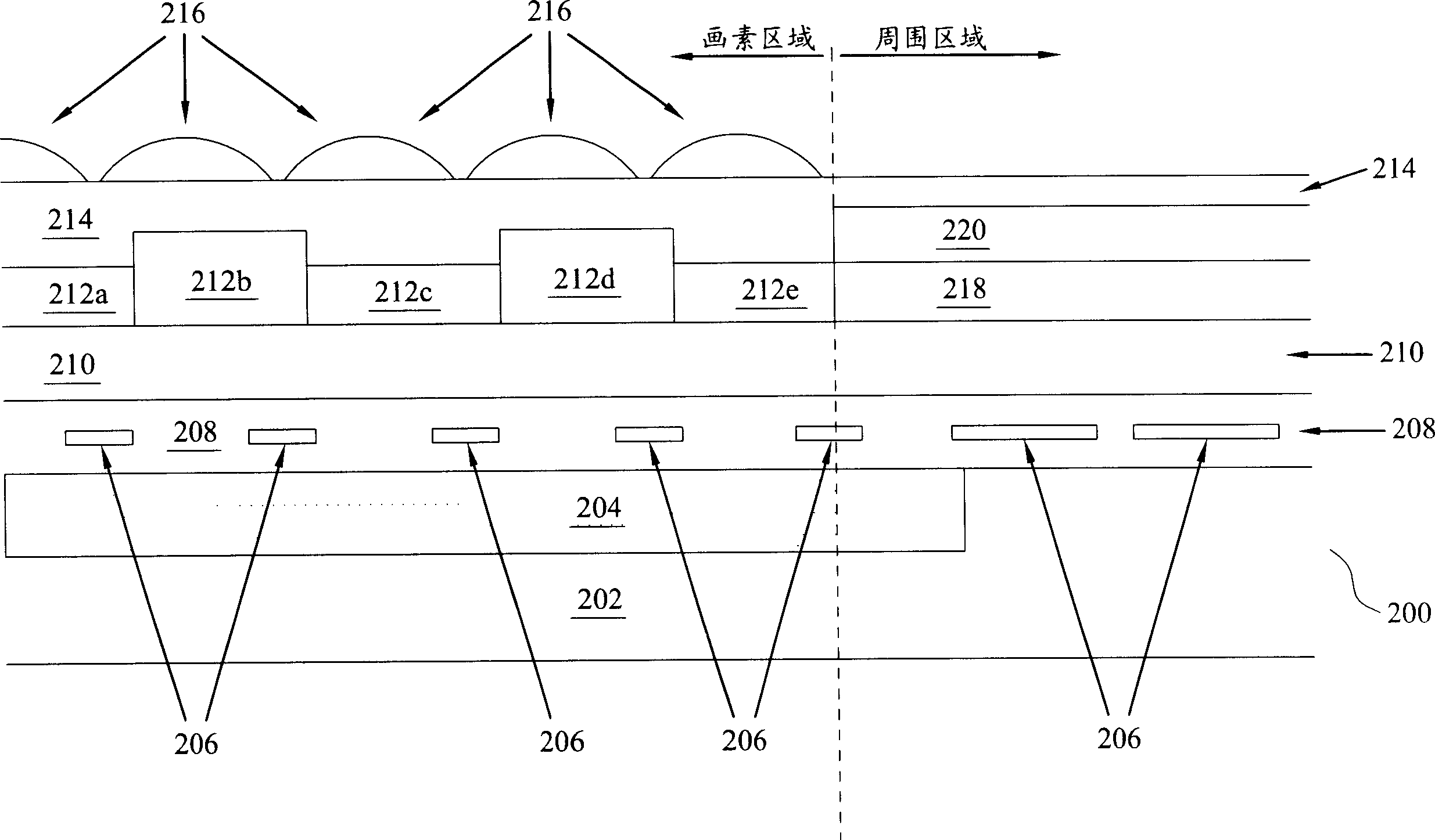
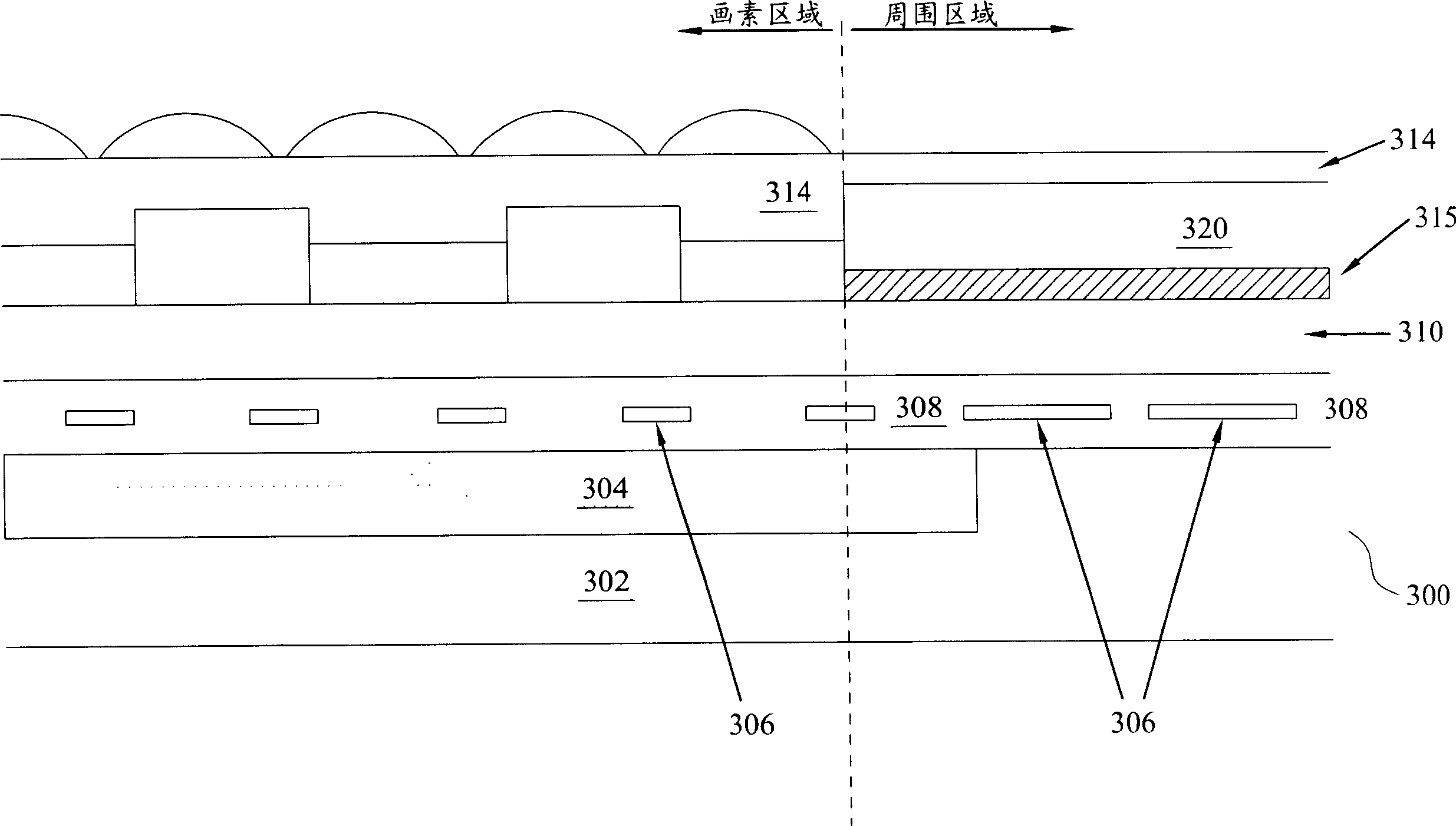
[0044] The present invention discloses an improved method and structure for enhancing noise immunity in a Complementary Metal Oxide Semiconductor Field Effect Transistor (CMOS) image sensor device. The present invention uses light blocking layers to further minimize and help eliminate stray and undesired light that causes electrical noise within the pixel array.

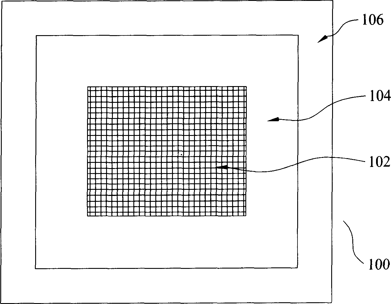
[0045] see figure 1 As shown, it is a top view showing main areas of a conventional CMOS image sensor (CIS) device 100 . The...


PUM


Abstract

A method and device is disclosed for reducing noise in CMOS image sensors. An improved CMOS image sensor includes a light sensing structure surrounded by a support feature section. An active section of the light sensing structure is covered by no more than optically transparent materials. A light blocking portion includes an opaque layer or a black light filter layer in conjunction with an opaque layer, covering the support feature section. The light blocking portion may also cover a peripheral portion of the light sensing structure. The method for forming the CMOS image sensors includes using film patterning and etching processes to selectively form the opaque layer and the black light filter layer where the light blocking portion is desired, but not over the active section. The method also provides for forming microlenses over the photosensors in the active section.

Description

technical field [0001] The present invention relates to the field of image devices, and in particular to the improvement of the noise immunity in the structure of a Complementary Metal Oxide Semiconductor Field Effect Transistor (CMOS) image sensor. Background technique [0002] Solid-state image sensors, such as charge-coupled devices (CCD) and complementary metal-oxide-semiconductor field-effect transistor (CMOS) image sensors (CIS), are often used as electronic video, still cameras, robot / machine vision and other input devices. These sensors include at least light-sensing elements (photodiodes) in individual pixels, and these pixels are arranged in a two-dimensional pixel array arranged in rows and columns. The light data received by the plurality of light-sensing pixels is processed together using associated logic and amplification circuits to generate an overall optical image as sensed by the pixel array. Each pixel may at least include a color filter on the light sen...

Claims


Application Information

Patent Timeline
Patent Type & Authority Applications(China)
IPC IPC(8): H01L27/146
CPCH01L27/14621H01L27/14623H01L27/14643H01L27/14685
Inventor 吴天启林宗毅
Owner TAIWAN SEMICON MFG CO LTD
Learn More