Multilayer antireflection coating of crystalline silicon cell and preparation method of multilayer antireflection coating

A technology of crystalline silicon cells and anti-reflection coatings, which is applied in the field of solar cells, can solve the problems of escaping from silicon wafers and the difference in refractive index is not obvious, and achieve the effects of good light transmission, improved light transmission, and fast short-wave response

Inactive Publication Date: 2017-02-22
庞倩桃
View PDF3 Cites 5 Cited by
  • Summary
  • Abstract
  • Description
  • Claims
  • Application Information

AI Technical Summary

Problems solved by technology

In addition, the silicon nitride film is a gradient film, the difference in refractive index between the film layer

Method used


Image

  • Multilayer antireflection coating of crystalline silicon cell and preparation method of multilayer antireflection coating

Examples


Embodiment Construction

[0016] The present invention will be further illustrated below in conjunction with the accompanying drawings and specific embodiments. This embodiment is implemented on the premise of the technical solution of the present invention. It should be understood that these embodiments are only used to illustrate the present invention and are not intended to limit the scope of the present invention.

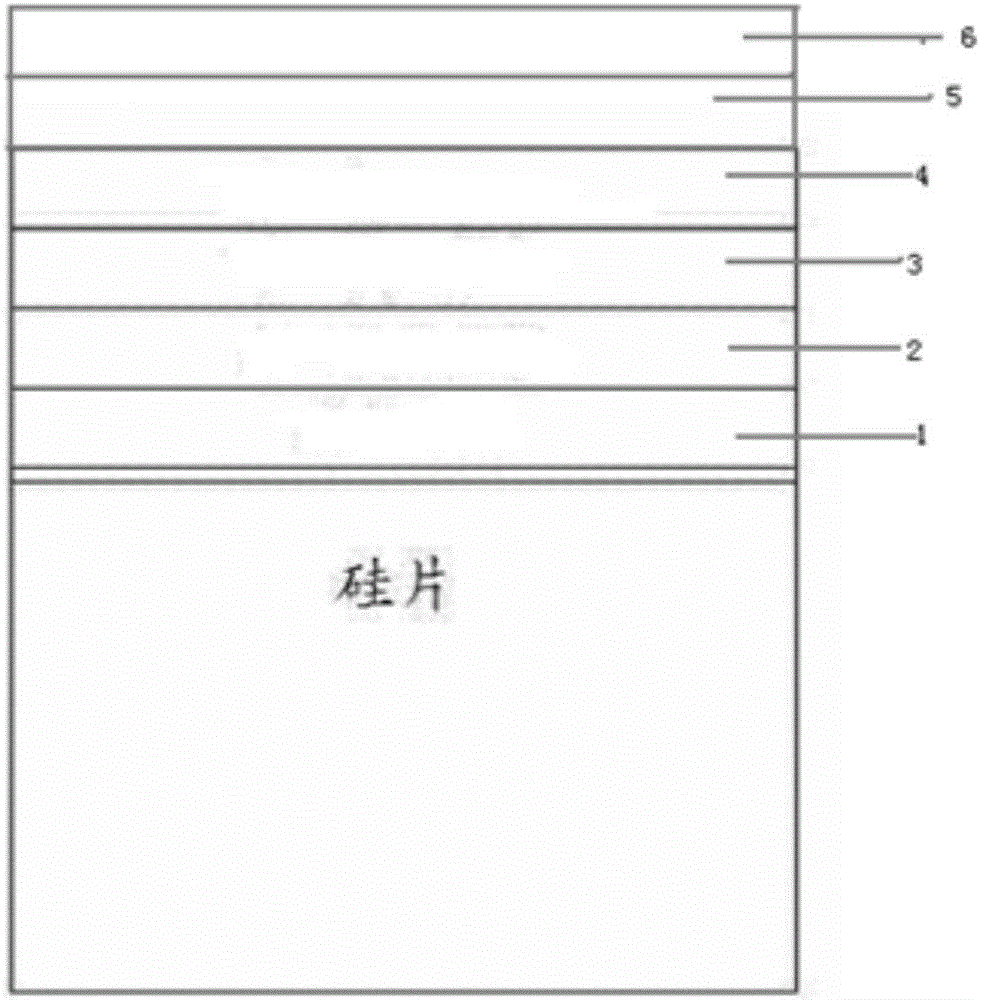
[0017] Such as figure 1 A multi-layer anti-reflection film for a crystalline silicon battery is shown, the anti-reflection film is deposited on the N-type surface of the crystalline silicon battery, and the anti-reflection film includes from bottom to top: a silicon oxide film 1, a first nitrogen Silicon nitride film 2, second silicon nitride film 3, third silicon nitride film 4, fourth silicon nitride film 5 and zirconium dioxide barrier layer 6, wherein the thickness of silicon oxide film 1 is 5-25nm, and the refractive index 1.4-1.5, the thickness of the first silicon nitride film 2 ...


PUM

PropertyMeasurementUnit
Thicknessaaaaaaaaaa
Thicknessaaaaaaaaaa
Thicknessaaaaaaaaaa

Abstract

The invention discloses a multilayer antireflection coating of a crystalline silicon cell. The multilayer antireflection coating deposits on an N-shaped side of the crystalline silicon cell and comprises a silicon oxide film, a first silicon nitride film, a second silicon nitride film, a third silicon nitride film, a fourth silicon nitride film and a zirconium dioxide barrier layer from bottom to top, wherein the silicon oxide film is 5-25 nanometers in thickness and 1.4-1.5 in refractive index, the first silicon nitride film is 6-12 nanometers in thickness and 2.25-2.35 in refractive index, the second silicon nitride film is 18-25 nanometers in thickness and 2.15-2.24 in refractive index, the third silicon nitride film is 35-55 nanometers in thickness and 2.05-2.14 in refractive index, the fourth silicon nitride film is 15-30 nanometers in thickness and 1.95-2.04 in refractive index, and the zirconium dioxide barrier layer is 30-50 nanometers in thickness. The multilayer antireflection coating of the crystalline silicon cell has the advantages of fast short wave response, low refractive index, excellent light permeability and the like.

Description

technical field [0001] The invention relates to the technical field of solar cells, in particular to a multilayer antireflection film for a crystalline silicon cell and a manufacturing method thereof. Background technique [0002] Potential-Induced Degradation (PID, Potential-Induced Degradation) is ubiquitous in traditional photovoltaic modules. According to the results of many domestic and foreign research institutions, the main reason for PID is: as the number of photovoltaic modules in series continues to increase, photovoltaic The probability that components will withstand high voltage-to-ground potential energy is also increasing. When one end of the system is grounded, the component farthest from the ground will generate a higher ground potential, which is close to 1000v in European design standards. Under such a high voltage, leakage current will be generated and power generation will be lost. The leakage current generally flows into the ground through the aluminum ...

Claims


Application Information

Patent Timeline
IPC IPC(8): H01L31/0216H01L31/068H01L31/18
CPCH01L31/02167H01L31/02168H01L31/068H01L31/1868Y02E10/547Y02P70/50
Inventor 庞倩桃
Owner 庞倩桃
Why Eureka
Try Eureka