Crystalline silicon solar cell and preparation method thereof

A technology of solar cells and crystalline silicon, applied in circuits, photovoltaic power generation, electrical components, etc., can solve the problems that the refractive index of thin-film aluminum oxide materials cannot be achieved, the application cannot be implemented, and cannot be implemented.

Inactive Publication Date: 2019-07-26
JIANGSU MICROVIA NANO EQUIP TECH CO LTD
View PDF5 Cites 3 Cited by
  • Summary
  • Abstract
  • Description
  • Claims
  • Application Information

AI Technical Summary

Problems solved by technology

This application still exists because the metallization process needs to be carried out on the plated film structure, that is, printing conductive silver paste and sintering and curing, but the aluminum oxide material used before the metallization process will block the penetration of the silver electrode, resulting in Problems with which this application cannot be implemented
In

Method used


Image

  • Crystalline silicon solar cell and preparation method thereof
  • Crystalline silicon solar cell and preparation method thereof
  • Crystalline silicon solar cell and preparation method thereof

Examples


Embodiment 1

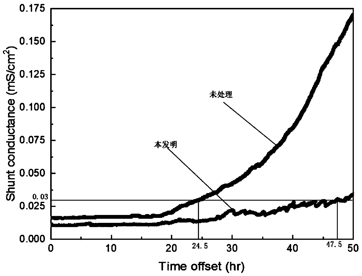
[0034] Embodiment 1 introduces a finished crystalline silicon solar cell that has not been treated by the present invention, and other embodiments will use it as a comparative example to prove the effect of the present invention. The test result curve is as figure 1 shown.

Embodiment 2-9

[0036] In Examples 2-9, PERC cells were double-sided Al by atomic layer deposition (ALD) equipment 2 o 3Coating, wherein the substrate temperature is 200°C, the pressure is 2-20mbar, the inert gas N 2 As carrier gas and purge gas, the flow rate is 400-2000sccm. Step ① uses trimethylaluminum as precursor A, the pulse duration is 0.5-3s; step ② uses N 2 Purification, the duration is 1-4s; step ③ uses water as precursor B, the duration is 1-4s; step ④ uses N 2 Purification, duration 2-6s. The plating rate was 0.12 nm / cycle. Alternate feed, grow layer by layer, control the number of cycles to reach the target thickness.

[0037] The Al obtained by ellipsometry 2 o 3 The refractive index of the film was tested, and the refractive index was 1.625.

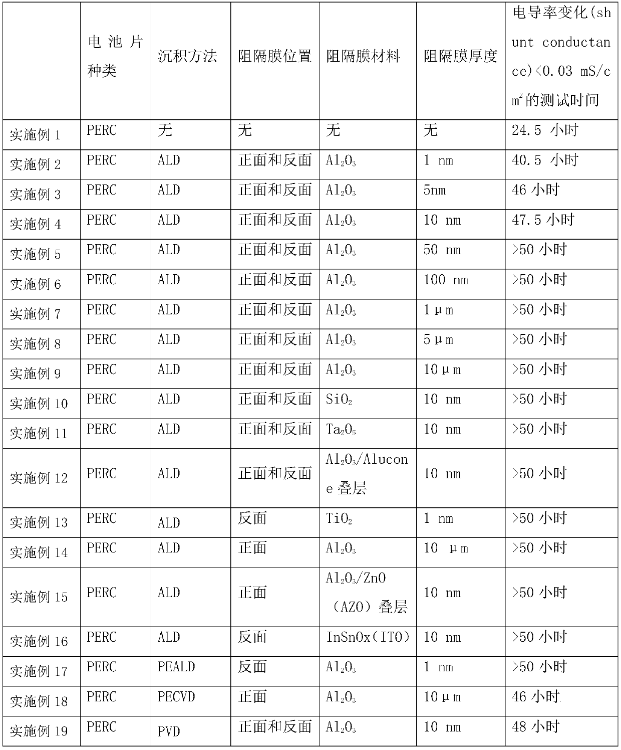
[0038] The anti-PID effect of the battery is shown in the corresponding part of Table 1. Wherein the test curve of embodiment 4 is as figure 1 shown.

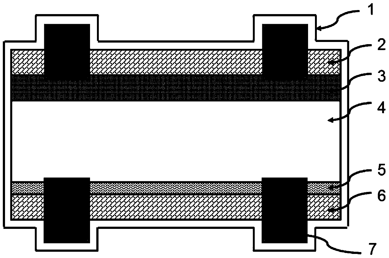
[0039] Gained crystalline silicon solar cell, its structure is as follows ...

Embodiment 10-16

[0041] In Examples 10-16, one or both sides of the PERC battery are coated with various materials as raw materials by atomic layer deposition (ALD) equipment, similar to Examples 2-9, wherein the substrate temperature is 200°C , the pressure is 2-20mbar, choose N 2 As carrier gas and purge gas, the flow rate is 400-2000sccm. Step ① use trimethylaluminum as precursor A, pulse duration 0.5-3s; step ② use N 2 Purification, duration 1-4s; step ③ use water as precursor B, duration 1-4s; step ④ use N 2 Purification, the duration of purification is 2-6s. Alternate feed, grow layer by layer, control the number of cycles to reach the target thickness. It can be adjusted according to different materials.

[0042] By controlling the deposition time, crystalline silicon solar cells with different barrier film thicknesses can be obtained, and the anti-PID effect is shown in the corresponding part of Table 1.


PUM

PropertyMeasurementUnit
Thicknessaaaaaaaaaa
Thicknessaaaaaaaaaa

Abstract

The invention relates to the field of photovoltaic cells, to be specific, relates to a crystalline silicon solar cell and a preparation method thereof. The invention is characterized in that a surfaceof a cell piece is provided with a barrier film; the surface of the finished cell piece is further provided with the barrier film in a coated manner to form an ion diffusion barrier layer, and one surface or two surfaces of the finished battery piece are wrapped to be used as a diffusion barrier layer for blocking external ions from migrating to the battery, and therefore, the PID resistance of the cell is improved, the passivation and anti-reaction effects are improved at the same time, and the photoelectric conversion efficiency of the battery is improved; the coating film on the surface ofthe cell piece can also be used for protecting the electrode from oxidation and resisting aging. ALD or PEALD technology is preferably used, and the dense pinhole-free performance of the ALD thin film is fully used to further improve the PID resistance of the cell.

Description

technical field [0001] The invention relates to the field of photovoltaic cells, in particular to a crystalline silicon solar cell and a preparation method thereof. Background technique [0002] Crystalline silicon and thin-film solar cells are increasingly used as renewable energy sources to replace traditional energy sources that have an impact on the environment. In grid power generation, many photovoltaic modules are connected in series to achieve the required voltage, and the frame of the modules is grounded. The components are exposed to high voltage for a long time, causing leakage between the packaging glass and other materials, causing a large amount of charge to accumulate on the surface of the battery, resulting in deterioration of the performance of the battery during use and a decrease in photoelectric conversion efficiency. This phenomenon is called Potential-Induced Degradation (PID), that is, the so-called voltage causes attenuation. This phenomenon is univ...

Claims


Application Information

Patent Timeline
IPC IPC(8): H01L31/0216H01L31/18
CPCH01L31/02167H01L31/02168H01L31/1804H01L31/1868Y02E10/547Y02P70/50
Inventor 黎微明李翔布莱姆·豪克斯
Owner JIANGSU MICROVIA NANO EQUIP TECH CO LTD
Why Eureka
Try Eureka