A method for aluminum gettering of ingot polycrystalline silicon wafer

A technology of polycrystalline silicon wafers and ingots, which is applied in the field of gettering process of ingot polycrystalline silicon wafers, can solve the problems of high carrier recombination activity, limiting the electrical properties of solar cells, etc., and achieve efficiency improvement, high industrial production value, and high stability sexual effect

Active Publication Date: 2018-05-01
HEBEI UNIV OF TECH
View PDF2 Cites 0 Cited by
  • Summary
  • Abstract
  • Description
  • Claims
  • Application Information

AI Technical Summary

Problems solved by technology

Due to the high carrier recombination activity of transition metals and their precipitates, the presence of such contamination limits the electrical performance of solar cells

Method used


Image

  • A method for aluminum gettering of ingot polycrystalline silicon wafer
  • A method for aluminum gettering of ingot polycrystalline silicon wafer

Examples


Embodiment 1

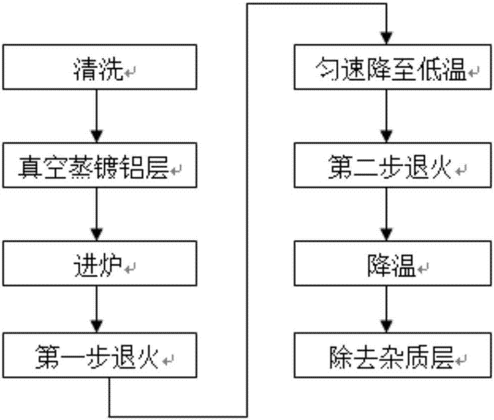
[0025] A method for aluminum gettering of cast polycrystalline silicon wafers, the specific process flow is as follows:

[0026] (1) Cleaning: The sample material is cast P-type polysilicon wafers, and the standard RCA solution cleaning method is used for cleaning: use No. Liquid HPM was ultrasonicated in a water bath at 80°C for 10 minutes to remove metal impurities;

[0027] (2) Vacuum evaporation aluminum layer: put the cleaned polysilicon wafer into the vacuum evaporation equipment, and vacuum the equipment to 7.5×10 4 Pa, aluminum is evaporated on the surface of the polycrystalline silicon wafer, and the thickness of the aluminum layer is 1.3 μm;

[0028] (3) Into the furnace: put the aluminized polysilicon wafer and the quartz boat together into the tubular annealing furnace, rush into the argon atmosphere, avoid pollution during the whole process, and raise the temperature of the tubular annealing furnace to 810°C at a uniform speed , the heating rate is 5°C / min;

[...

Embodiment 2

[0036] A method for aluminum gettering of cast polycrystalline silicon wafers, the specific process flow is as follows:

[0037] (1) Cleaning: The sample material is cast P-type polysilicon wafers, and the standard RCA solution cleaning method is used for cleaning: use No. Liquid HPM was ultrasonicated in a water bath at 80°C for 10 minutes to remove metal impurities;

[0038] (2) Vacuum evaporation aluminum layer: put the cleaned polysilicon wafer into the vacuum evaporation equipment, and vacuum the equipment to 7.5×10 4 Pa, aluminum is evaporated on the surface of the polycrystalline silicon wafer, and the thickness of the aluminum layer is 1.5 μm;

[0039] (3) Into the furnace: Put the aluminum-coated polycrystalline silicon wafer and the quartz boat together into the tubular annealing furnace, rush into the argon atmosphere, avoid pollution during the whole process, and raise the temperature of the tubular annealing furnace to 830°C at a uniform speed , the heating rate...


PUM

PropertyMeasurementUnit
thicknessaaaaaaaaaa

Abstract

The invention discloses an aluminium gettering method for ingot polycrystalline silicon chips. The method comprises the following main steps of (1) cleaning; (2) vacuum evaporation of an aluminium layer; (3) into a furnace; (4) first annealing; (5) cooling at a constant speed to low temperature; (6) second annealing; (7) cooling; (8) removal of an impurity layer. After a large number of experimental verification, the process of the invention can remove most of the metal impurities (such as iron, nickel, copper, cobalt and the like) in the ingot polycrystalline silicon chips, thereby increasing the lifetime of the minority carrier to improve the photoelectric conversion efficiency of the solar cell. The average minority carrier lifetime of the polycrystalline silicon chips subjected to the aluminium gettering is determined to be about 15.80 [mu]s by an apparatus, and the aluminium gettering process of the present invention is relatively stable and had a high industrial production value.

Description

technical field [0001] The invention relates to a gettering process of cast polycrystalline silicon wafers, in particular to a method for aluminum gettering of cast polycrystalline silicon wafers. Background technique [0002] As a new energy source, solar energy has become a vigorously developed industry in the 21st century. A large part of the cost of solar cells is consumed by the raw material for producing cells - Si. The purity of the silicon material used in solar cells must be above 99.9999% (6N), which is electronic grade silicon (EG Si) obtained from metallurgical grade silicon (UMG Si) through complex purification methods, which is an important reason for cost consumption. [0003] There are many transition group metal impurities and defects in polysilicon, such as: iron, nickel, copper and cobalt. These impurities severely reduce the minority carrier lifetime by forming recombination centers in the band gap. Due to the high carrier recombination activity of tra...

Claims


Application Information

Patent Timeline
Patent Type & Authority Patents(China)
IPC IPC(8): H01L31/18H01L21/322
CPCH01L21/3221H01L31/1804Y02E10/547Y02P70/50
Inventor 张辉解新建陈贵锋常雪岩阎文博陶俊光
Owner HEBEI UNIV OF TECH
Why Eureka
Try Eureka