Organic electroluminescent device and preparation method thereof

An electroluminescence device and luminescence technology, which is applied in the manufacture of organic semiconductor devices, electric solid state devices, semiconductor/solid state devices, etc., can solve the problems of changing the light emitting properties of the light emitting layer, low external quantum efficiency, uncontrollable light emitting properties, etc.

Inactive Publication Date: 2017-02-22
SOUTH UNIVERSITY OF SCIENCE AND TECHNOLOGY OF CHINA +1
View PDF10 Cites 31 Cited by
  • Summary
  • Abstract
  • Description
  • Claims
  • Application Information

AI Technical Summary

Problems solved by technology

The light-emitting layer of the light-emitting diode adopts CsPbX 3 , the light-emitting properties of the light-emitting layer can be adjusted by X being a combination of any two of Cl, Br and I, but the simple doping of the two compounds does not have much impact on the light-emitting layer, and cannot fundamentally change the light-emitting properties of the light-emitting layer, And it is easy to cause the problem of uneven luminescence, and the external quantum efficiency is low
[0006] Therefore, for the light-emitting layer of organic electroluminescent devices in the prior art, quantum dots such as CdSe and CdS are used, the quantum efficiency is low, and the light-emitting properties are uncontrollable; If it has too much influence, it cannot fundamentally change the luminescent properties of the luminescent layer, and it is easy to cause uneven luminescence. It is very important to study a new organic electroluminescent device.

Method used


Image

  • Organic electroluminescent device and preparation method thereof

Examples


preparation example Construction

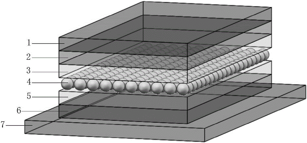
[0069] The specific embodiment part of the present invention also provides a preparation method of the organic electroluminescence device, and the preparation method includes the following steps:

[0070] (1) Spin-coat the hole injection material on the coating surface of the anode, and solidify to obtain the hole injection layer 6;

[0071] (2) Spin-coat the hole transport material on the surface of the hole injection layer 6 obtained in step (1), and solidify to obtain the hole transport layer 5;

[0072] (3) Spin-coat perovskite quantum dots on the surface of the hole transport layer 5 obtained in step (2), and solidify to obtain the light-emitting layer 4;

[0073] (4) The surface of the luminescent layer 4 obtained in step (3) is coated with an electron transport material, an electron injection material and a cathode material in sequence to obtain an organic electroluminescent device.

[0074] For better illustrating the present invention, facilitate understanding techni...

Embodiment 1

[0076] A preparation method of an organic electroluminescent device, the preparation method comprising the following steps:

[0077] (1) Spin-coat a layer of polythienothiophene doped with poly(perfluoroethylene-perfluoroethersulfonic acid) with a thickness of 20nm on the surface of the indium tin oxide coating of conductive glass. The speed of spin coating is 4000rpm, and the spin coating The time is 60s, and the spin coating is baked at 115° C. for 15 minutes to cure, and the hole injection layer 6 is obtained;

[0078] (2) The surface of the hole injection layer 6 obtained in step (1) is spin-coated with 18nm thick poly[N,N'-bis(4-butylphenyl)-N,N'-bis(phenyl)benzidine ], the spin-coating speed is 4000rpm, the spin-coating time is 35s, and the spin-coating layer is baked at 115°C for 15min to cure and solidify to obtain the hole transport layer 5;

[0079] (3) spin-coat 25nm thick perovskite type CsPbCl on the hole transport layer 5 surface that step (2) obtains 0.9 I 2....

Embodiment 2

[0083] A preparation method of an organic electroluminescent device, the preparation method comprising the following steps:

[0084] (1) Spin-coat a layer of nickel oxide with a thickness of 10nm on the surface of the fluorine-doped tin oxide coating of conductive glass, the speed of spin coating is 3000rpm, the time of spin coating is 40s, and the spin coating is baked at 100°C for 25min to solidify. A hole injection layer 6 is obtained;

[0085] (2) The surface of hole injection layer 6 obtained in step (1) is spin-coated with 5nm thick NPD, the speed of spin coating is 3000rpm, the time of spin coating is 20s, and the spin coating is baked at 100°C for 25min to cure and solidify. A hole transport layer 5 is obtained;

[0086] (3) spin-coat 10nm thick perovskite type CsPbCl on the hole transport layer 5 surface that step (2) obtains 1.1 Br 1.9 For quantum dots, the speed of spin coating is 1000rpm, the time of spin coating is 20s, and the spin coating is baked at 100°C fo...


PUM


Abstract

The invention relates to an organic electroluminescent device. The organic electroluminescent device comprises a hole injection layer (6), a hole transmission layer (5), a luminescent layer (4), an electronic transmission layer (3), an electronic injection layer (2) and a cathode layer (1) which are connected sequentially from one side of an anode layer (7), wherein the luminescent layer is a perovskite type quantum dot; the perovskite type quantum dot is CsPbXaYb; and X comprises any one of Cl, Br or I, Y comprises any one of Cl, Br or I, X and Y are different, a is more than 0, b is more than 0, and a plus b is equal to 3. The organic electroluminescent device can regulate and control the luminescent property by controlling the proportion of luminescent layer perovskite type quantum dot halogen, and is high in brightness, small in starting voltage and simple in preparation process.

Description

technical field [0001] The invention relates to the field of optoelectronics, and relates to a photoelectric device and a preparation method thereof, in particular to an organic electroluminescent device and a preparation method thereof. Background technique [0002] At present, the electroluminescent device is a kind of self-luminous device, which belongs to injection light emission. Under the action of forward bias, the anode injects holes into the charge transport layer, and moves to the interface of the transport layer under the action of the electric field, while the cathode The injected electrons also move from the electron transport layer to the interface. Due to the effect of the potential barrier, the electrons are not easy to enter the charge transport layer, but accumulate on the side of the light-emitting layer near the interface. The electrons injected from the cathode and the holes injected from the anode are in the light-emitting layer. Meet, recombine, releas...

Claims


Application Information

Patent Timeline
Patent Type & Authority Applications(China)
IPC IPC(8): H01L51/50H01L51/56
CPCH10K50/115H10K2102/351H10K71/00
Inventor 王恺孙小卫刘皓宸刘培朝曹万强郝俊杰周子明
Owner SOUTH UNIVERSITY OF SCIENCE AND TECHNOLOGY OF CHINA
Why Eureka
Try Eureka