Carrier-Attached Copper Foil, Laminate, Method For Producing Printed Wiring Board, And Method For Producing Electronic Device

A technology of copper foil with carrier and printed wiring board, which is applied in the fields of printed circuit manufacturing, printed circuit, electronic equipment, etc., can solve the problem of reduced adhesion and achieve the effect of fine circuit formation

Active Publication Date: 2017-02-22
JX NIPPON MINING & METALS CORP
View PDF48 Cites 9 Cited by
  • Summary
  • Abstract
  • Description
  • Claims
  • Application Information

AI Technical Summary

Problems solved by technology

The adhesion (peel strength) of the ultra-thin copper layer without such roughening treatment to resin is inferior to that of general copper foil for printed wiring boards due to the influence of the low distribution (concave-convex, roughness, roughness). Tendency to decrease specific adhesion

Method used

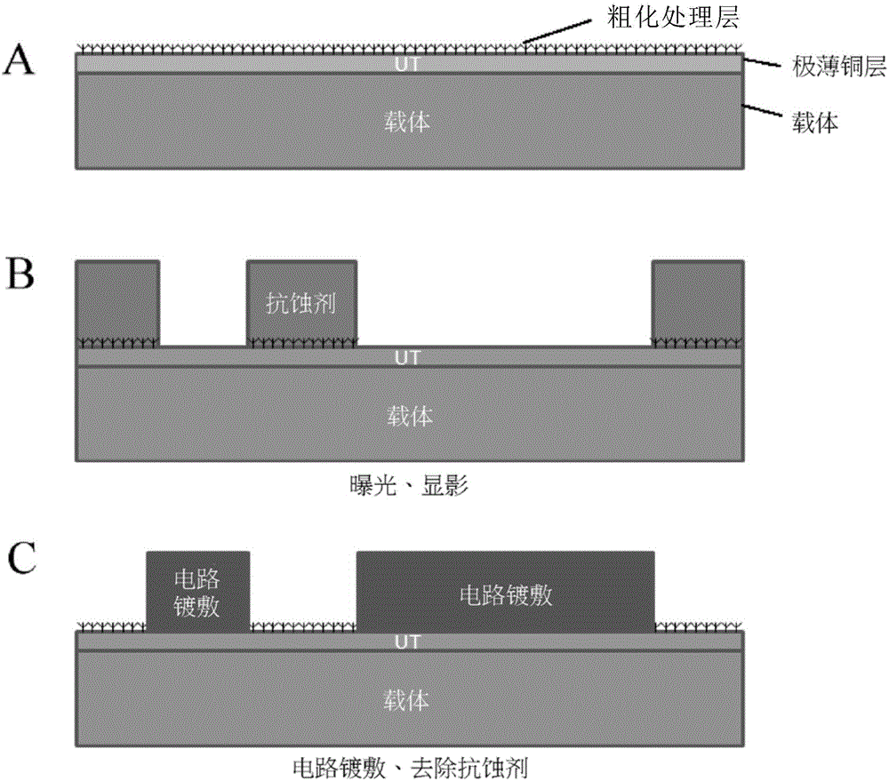
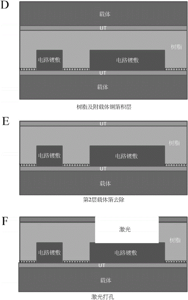
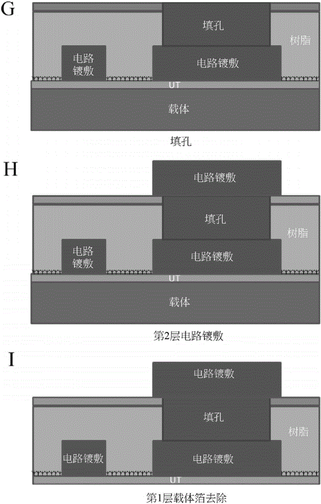

Image

  • Carrier-Attached Copper Foil, Laminate, Method For Producing Printed Wiring Board, And Method For Producing Electronic Device
  • Carrier-Attached Copper Foil, Laminate, Method For Producing Printed Wiring Board, And Method For Producing Electronic Device
  • Carrier-Attached Copper Foil, Laminate, Method For Producing Printed Wiring Board, And Method For Producing Electronic Device

Examples


Embodiment

[0487] Hereinafter, the present invention will be described in further detail through examples of the present invention, but the present invention is not limited by these examples.

[0488] (1) Production of carrier

[0489] First, a carrier is fabricated as follows.

[0490] ・Carrier production method A (Examples 1 to 3, Comparative Examples 1 and 5)

[0491] As the smooth polyimide film, Ube Industries, Ltd. Upilex SGA (BPDA-PPD polyimide film) having a thickness of 25 μm was used as a carrier. Then, the surface of the smooth polyimide film on the side where the ultra-thin copper layer is scheduled to be provided was subjected to plasma treatment in the following manner. After the smooth polyimide film is placed in the vacuum device and vacuum exhausted, oxygen is introduced into the chamber, and the pressure of the chamber is adjusted to 5-12Pa. Thereafter, the power of the plasma treatment is set to 100 to 200 W, and the plasma treatment is performed for 20 to 40 second...

Embodiment 4

[0498] The production method B of the carrier (embodiment 4, embodiment 11)

[0499] A titanium drum (electrolysis drum) was prepared, and as the surface control conditions of the electrolysis drum, the surface of the electrolysis drum was ground with a grinding wheel abrasive particle size: #3000, and a grinding wheel rotation speed: 500 rpm. Next, the electrolytic drum is arranged in the electrolytic cell, and electrodes are arranged around the drum with a predetermined inter-electrode distance therebetween. Next, electrolysis was performed in the electrolytic cell under the following conditions, and copper was deposited on the surface of the electrolytic drum while rotating the electrolytic drum.

[0500]

[0501] Copper: 80~110g / L

[0502] Sulfuric acid: 70~110g / L

[0503] Chlorine: 10-100 mass ppm

[0504]

[0505] Current density: 50~200A / dm 2

[0506] Electrolyte temperature: 40~70℃

[0507] Electrolyte linear velocity: 3~5m / sec

[0508] Electrolysis time: 0....

Embodiment 8

[0528]A titanium drum (electrolysis drum) was prepared, and as the surface control conditions of the electrolysis drum, the surface of the electrolysis drum was ground at a grinding wheel abrasive particle size: #1000, and a grinding wheel rotation speed: 500 rpm. Next, the electrolytic drum is arranged in the electrolytic cell, and electrodes are arranged around the drum with a predetermined inter-electrode distance therebetween. Next, electrolysis was performed in the electrolytic cell under the following conditions, and copper was deposited on the surface of the electrolytic drum while rotating the electrolytic drum.

[0529]

[0530] Copper: 80~110g / L

[0531] Sulfuric acid: 70~110g / L

[0532] Chlorine: 10-100 mass ppm

[0533]

[0534] Current density: 50~200A / dm 2

[0535] Electrolyte temperature: 40~70℃

[0536] Electrolyte linear velocity: 3~5m / sec

[0537] Electrolysis time: 0.5 to 10 minutes

[0538] Next, the copper deposited on the surface of the rotatin...


PUM

PropertyMeasurementUnit
thicknessaaaaaaaaaa
thicknessaaaaaaaaaa
thicknessaaaaaaaaaa

Abstract

Provided herein is a carrier-attached copper foil having desirable fine circuit formability. The carrier-attached copper foil includes a carrier, an interlayer, and an ultrathin copper layer in this order, wherein D2-D1 is 0.30 to 3.83 [mu]m, where D1 is the gravimetrically measured thickness of the carrier-attached copper foil excluding the carrier and the interlayer, and D2 is the maximum thickness of the layer remaining on a bismaleimide-triazine resin substrate in case of detaching the carrier after the carrier-attached copper foil is laminated to the resin substrate from the ultrathin copper layer side by being heat pressed under a pressure of 20 kgf / cm2 at 220 DEG C for 2 hours.

Description

technical field [0001] The present invention relates to a method for manufacturing copper foil with a carrier, a laminate, a printed wiring board, and an electronic device. Background technique [0002] A printed wiring board is usually produced through a step of forming a conductive pattern on the surface of the copper foil by etching after bonding an insulating substrate to copper foil to form a copper-clad laminate. With the increasing demand for miniaturization and high performance of electronic equipment in recent years, high-density mounting of mounted parts or high frequency of signals has been continuously developed, and the miniaturization of conductor patterns (fine pitch) is required for printed wiring boards. ) or high-frequency response, etc. [0003] In response to fine-pitching, the industry currently requires copper foil with a thickness of 9 μm or less, and a further thickness of 5 μm or less. However, due to the low mechanical strength of this type of ultr...

Claims


Application Information

Patent Timeline
Patent Type & Authority Applications(China)
IPC IPC(8): H05K3/02
CPCH05K3/025H05K3/0035H05K3/007H05K3/108H05K2201/0355H05K2203/0307H05K2203/0376H05K2203/0384B32B15/08B32B15/20B32B27/281B32B43/006C25D1/04C25D7/0614H05K1/09B32B2311/24B32B2457/08H05K3/4611H05K3/4661H05K3/4682H05K2203/06
Inventor 宫本宣明
Owner JX NIPPON MINING & METALS CORP
Why Eureka
Try Eureka