Laser marking device and method thereof

A printing device and laser technology, applied in laser welding equipment, electrical components, welding/welding/cutting items, etc., can solve the problems of unrecorded status, incapable of real-time inspection and post-inspection, increase of wafer yield change, etc., to achieve damage reduction effect

Inactive Publication Date: 2017-03-08
E&R ENG CORP
View PDF7 Cites 9 Cited by
  • Summary
  • Abstract
  • Description
  • Claims
  • Application Information

AI Technical Summary

Problems solved by technology

[0007] However, because the flattening device needs to be removed and then flattened again in order to rotate the wafer during processing, the surface of the wafer is pressed multiple times, thereby increasing the variation of the wafer yield; Unrecorded status, resulting in no real-time prosecution and post-mortem inspection

Method used


Image

  • Laser marking device and method thereof
  • Laser marking device and method thereof
  • Laser marking device and method thereof

Examples


Embodiment Construction

[0039] The present invention will be described in detail below in conjunction with the accompanying drawings and embodiments.

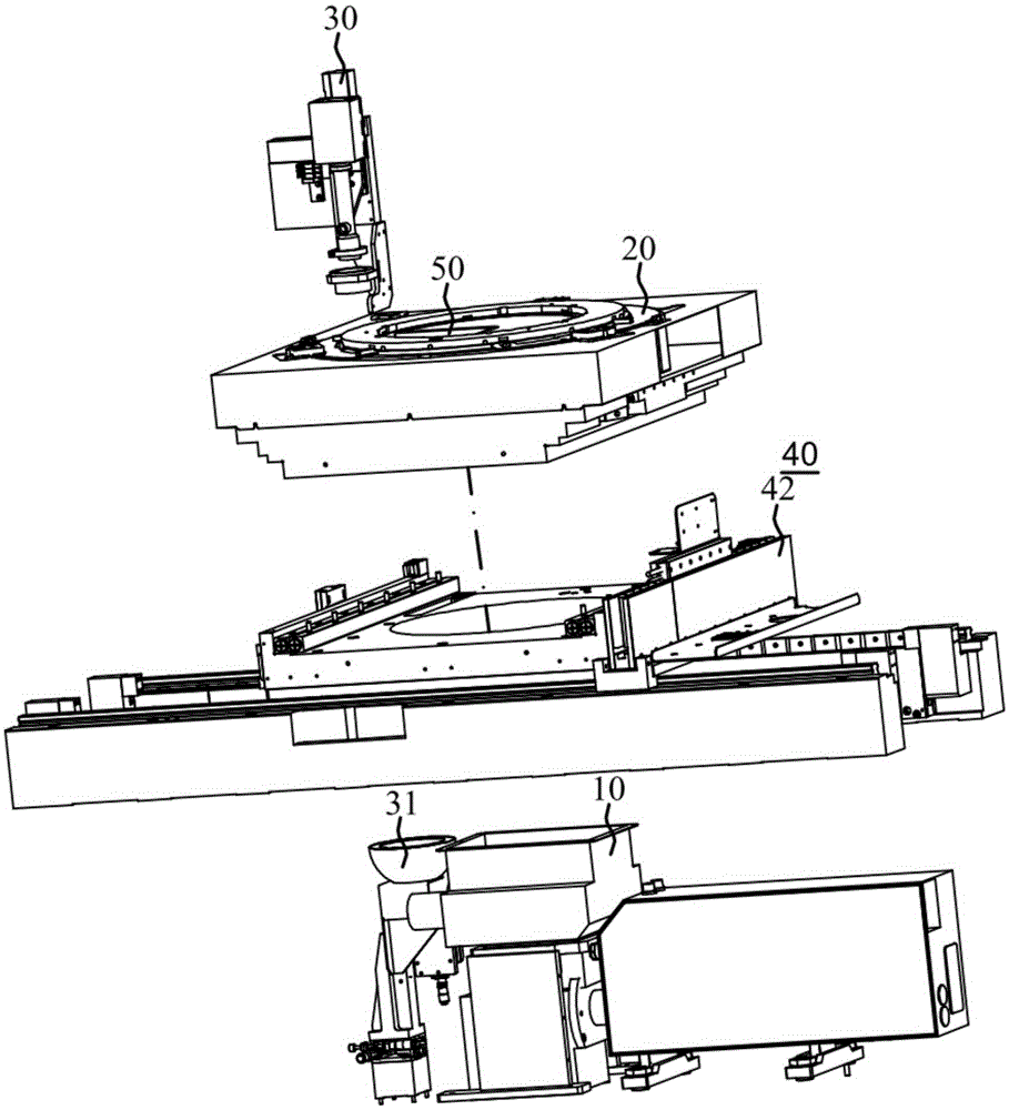
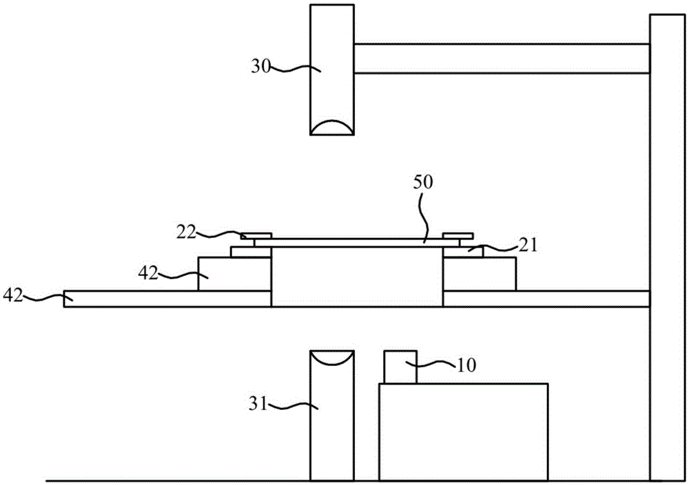
[0040] Such as Figure 1 to Figure 12 Shown is a laser printing device and its method provided by the present invention. Such as figure 1 As shown, the apparatus of the present invention includes a laser system 10 , a wafer leveling system 20 , a first imaging system 30 and a moving system 40 .

[0041] The laser system 10 refers to a laser (Light Amplification by Stimulated Emission of Radiation, LASER) generating device, which is mainly composed of three elements: the excitation source, the gain medium, and the resonant structure. It is very widely used in the precision processing and semiconductor industries due to its non-processing stress and precise characteristics. Generally, dust collection devices are provided around to collect the dust generated by processing.

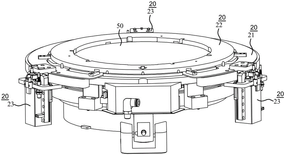
[0042] Such as Figure 5 , Figure 6As shown, the wafer leveling system 20 ...


PUM


Abstract

The present disclosure relates to a laser marking device and a method thereof. The laser marking device comprises a laser system, a wafer leveling system, a first imaging system and a mobile system: the wafer leveling system carries and levels a warped wafer to be processed; the mobile system underneath properly adjusts a position of the wafer; the first imaging system detects the wafer to recognize a product category and positioning status; the laser system underneath labels laser marks on the wafer; all wafers are marked in the cyclic process.

Description

technical field [0001] The invention relates to a wafer printing processing device and its method, in particular to a laser printing device and its method for performing laser printing operations under the condition of flattening the wafer. Background technique [0002] In recent years, smart phones have been regarded as a part of life by consumers, and various wearable devices are becoming more and more accepted. Corresponding to these consumer product trends, we can clearly understand that products tend to be miniaturized and have powerful computing capabilities change. Moreover, these consumer goods are basically electronic devices. The fastest way to make electronic devices smaller and increase their computing power is to improve the manufacturing process, and this type of theory is most famous for "Moore's Law"; among them, in the semiconductor manufacturing process One of the laser marking processes is to use a laser beam to mark the surface of the wafer for subsequen...

Claims


Application Information

Patent Timeline
Patent Type & Authority Applications(China)
IPC IPC(8): H01L21/66H01L23/544H01L21/67
CPCH01L21/67282H01L22/20H01L23/544H01L21/67288H01L21/68785B23K26/355B23K2103/56H01L21/268
Inventor 吴文仁钟卓君
Owner E&R ENG CORP
Why Eureka
Try Eureka