Lithium tantalate micro-patterning method based on reactive ion etching
A technology of reactive ion etching and lithium tantalate, which is applied in the manufacture of electrical components, semiconductor/solid-state devices, circuits, etc., can solve the problems of large stress and easy damage of patterns, and achieve easy fabrication and easy magnetron sputtering coating The effect of simple process and photolithography process
- Summary
- Abstract
- Description
- Claims
- Application Information
AI Technical Summary
Problems solved by technology
Method used
Image
Examples
Embodiment 1
[0042] A lithium tantalate micropatterning method based on reactive ion etching, comprising the steps of:
[0043] (1) cleaning the lithium tantalate substrate 1;
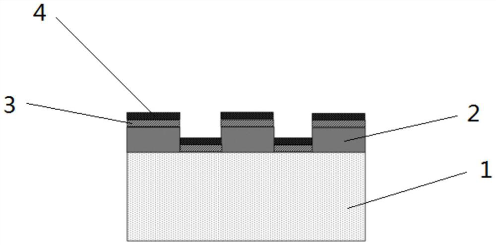
[0044] (2) Coating photoresist 2 on lithium tantalate substrate 1, exposing and developing to obtain patterned photoresist 2;
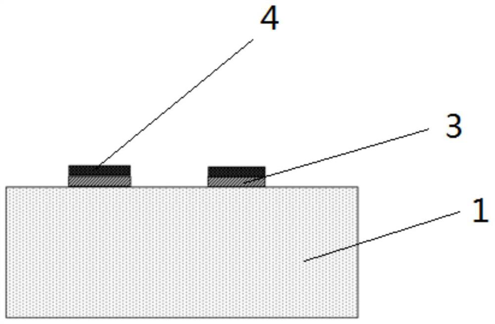
[0045] (3) Ti metal mask 3 and Cr metal mask 4 are sequentially plated with magnetron sputtering method on the photoresist 2 surface, the thickness of Ti metal mask 3 is 100nm, and the thickness of Cr metal mask 4 is 300nm;
[0046](4) Place the sample in step (3) in an acetone solution by stripping method to remove photoresist 2 and redundant metal parts, to obtain a patterned metal mask;
[0047] (5) Using CHF3 plasma to carry out 3min reactive ion etching on the lithium tantalate substrate 1 prepared with the metal mask pattern, the flow rate of the etching of the fluorine-based plasma is 50 sccm;
[0048] (6) Argon plasma is used to physically bombard the lithium tantalate substrate ...
Embodiment 2
[0053] On the basis of embodiment 1, in step (2), the thickness of Ti metal mask 3 is 20nm, and the thickness of Cr metal mask 4 is 50nm; Adopt CHF in step (5) The flow rate ratio with Ar plasma is 50sccm: 50sccm is carried out 1min reactive ion etching to the lithium tantalate substrate 1 that has prepared metal mask pattern; In step (6), adopt argon plasma to carry out 30s physical bombardment to lithium tantalate substrate 1, the flow rate during Ar physical bombardment is 50sccm, Repeat once, and the total time is 1.5 min; the rest of the steps are the same as in Example 1.
[0054] In this example, a trench pattern with a depth of 400 nm was produced.
Embodiment 3
[0056] On the basis of embodiment 1, on the basis of embodiment 1, the thickness of Ti metal mask 3 is 200nm in step (2), and the thickness of Cr metal mask 4 is 500nm; Adopt CF4 and Ar in step (5) The flow rate ratio of the plasma is 50sccm: 50sccm carries out 5min reactive ion etching to the lithium tantalate substrate 1 of metal mask pattern; Adopt argon plasma to carry out 2min physical bombardment to lithium tantalate substrate 1 in step (6), Ar The flow rate during the physical bombardment was 50 sccm, repeated four times, and the total time was 28 minutes; the rest of the steps were the same as in Example 1.
[0057] In this example, a groove pattern with a depth of 1.3 μm was produced.
PUM
| Property | Measurement | Unit |
|---|---|---|
| thickness | aaaaa | aaaaa |
| thickness | aaaaa | aaaaa |
| thickness | aaaaa | aaaaa |
Abstract
Description
Claims
Application Information


