Supercharge Your Innovation With Domain-Expert AI Agents!

Formation method for metal interconnecting structure

A metal interconnection, metal technology, applied in the direction of semiconductor/solid-state device components, electrical components, circuits, etc., can solve the problems of RC delay, electromigration, the performance of metal interconnection structure needs to be improved, etc., to improve performance, reduce resistance, The effect of alleviating the RC delay problem

Active Publication Date: 2017-03-08
SEMICON MFG INT (BEIJING) CORP +1
View PDF3 Cites 7 Cited by
  • Summary
  • Abstract
  • Description
  • Claims
  • Application Information

AI Technical Summary

Problems solved by technology

[0005] However, in the metal interconnection structure formed by the existing method, the resistance of the metal nitride barrier layer is relatively high, resulting in an increase in the resistance between the back metal and the front metal, which in turn causes serious RC delay problems
However, if the metal nitride barrier layer is not provided, copper is easy to diffuse into the dielectric layer, resulting in problems such as electromigration (EM)
Therefore, the performance of the existing metal interconnection structure needs to be improved

Method used


Image

  • Formation method for metal interconnecting structure
  • Formation method for metal interconnecting structure
  • Formation method for metal interconnecting structure

Examples


Embodiment Construction

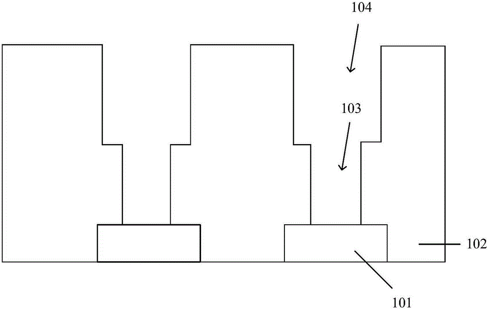
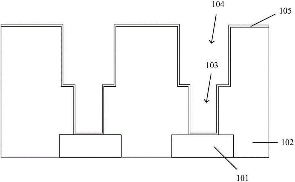
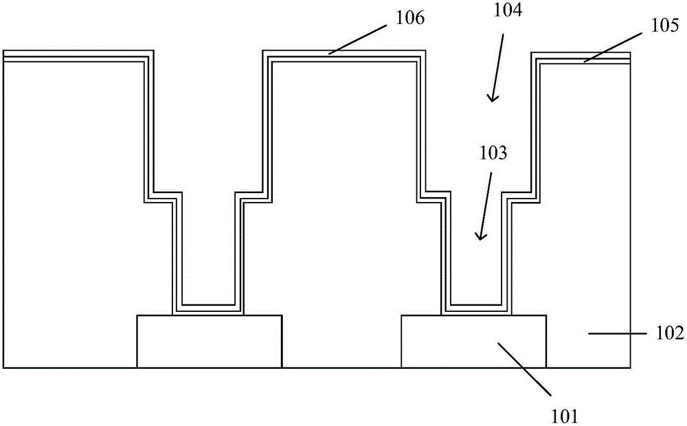
[0029] As mentioned in the background, in the existing semiconductor formation method, a metal nitride barrier layer is usually formed to prevent copper from diffusing into the dielectric layer. In the existing forming method, after forming the contact hole and the trench, the metal nitride barrier layer is directly formed. However, after the contact holes and trenches are formed, there will be many impurities on the surface of the front layer metal exposed at the bottom of the contact holes. These impurities are usually produced by the formation process of the contact holes and trenches. These impurities are usually nitrogen or oxygen elements. . When these impurities are present, the metal nitride barrier layer will cover them on the previous metal surface if the metal nitride barrier layer is formed directly. When subsequent layer metal is filled in the contact holes and trenches, these impurities still exist and cannot be eliminated. These impurities will lead to a decre...


PUM


Abstract

Disclosed is a formation method for a metal interconnecting structure. The formation method comprises the steps of providing a semiconductor substrate, wherein the semiconductor substrate is provided with front layer metal and a dielectric layer for covering the front layer metal; forming contact holes and trenches in the dielectric layer, wherein the front layer metal is exposed from the bottoms of the contact holes, the contact holes are connected with the trenches, and the trenches are formed above the corresponding contact holes; forming a first metal barrier layer on the inner walls of the contact holes and the inner walls of the trenches; forming a metal nitride barrier layer on the inner walls of the contact holes and the inner walls of the trenches, wherein the metal nitride barrier layer covers the first metal barrier layer; and after forming the metal nitride barrier layer, filling the contact holes and the trenches with back layer metal. By adoption of the formation method, the performance of the metal interconnecting structure is improved.

Description

technical field [0001] The invention relates to the field of semiconductor manufacturing, in particular to a method for forming a metal interconnection structure. Background technique [0002] With the continuous improvement of integrated circuit manufacturing technology, the volume of semiconductor devices is becoming smaller and smaller, and the parasitic capacitance between metals is getting larger and larger. The problem of resistance-capacitance (RC) delay is becoming more and more prominent. In order to solve the problem of RC delay, in terms of reducing resistance, since the resistance of copper is lower than that of aluminum, the industry uses copper interconnection technology to replace the original aluminum interconnection process. [0003] In the integrated circuit of the traditional aluminum interconnection process, the metal wire is made by etching the metal layer, and then the filling of the dielectric layer and the chemical mechanical polishing (Chemical Mecha...

Claims


Application Information

Patent Timeline
Patent Type & Authority Applications(China)
IPC IPC(8): H01L21/768
CPCH01L21/76883H01L23/5226H01L21/76843H01L21/76865H01L23/53238H01L21/76846H01L21/76804H01L21/76859H01L23/5283H01L23/53295
Inventor 刘继全
Owner SEMICON MFG INT (BEIJING) CORP
Features
  • R&D
  • Intellectual Property
  • Life Sciences
  • Materials
  • Tech Scout
  • Unparalleled Data Quality
  • Higher Quality Content
  • 60% Fewer Hallucinations
Learn More