Check patentability & draft patents in minutes with Patsnap Eureka AI!

Gene sequencing chip, gene sequencing apparatus and gene sequencing method

A gene sequencing and chip technology, which is applied to biochemical equipment and methods, measuring devices, and microbial measurement/inspection, etc., can solve problems such as high cost and complicated manufacturing process, and achieve simple manufacturing process, simple and convenient gene sequencing, and reduce Effects of Manufacturing Difficulty and Cost

Pending Publication Date: 2017-03-15
BOE TECH GRP CO LTD +1
View PDF3 Cites 26 Cited by
  • Summary
  • Abstract
  • Description
  • Claims
  • Application Information

AI Technical Summary

Problems solved by technology

Existing gene sequencing chips need to be masked, exposed, developed and etched multiple times during the manufacturing process, the manufacturing process is complicated and the cost is high

Method used


Image

  • Gene sequencing chip, gene sequencing apparatus and gene sequencing method
  • Gene sequencing chip, gene sequencing apparatus and gene sequencing method
  • Gene sequencing chip, gene sequencing apparatus and gene sequencing method

Examples


Embodiment 1

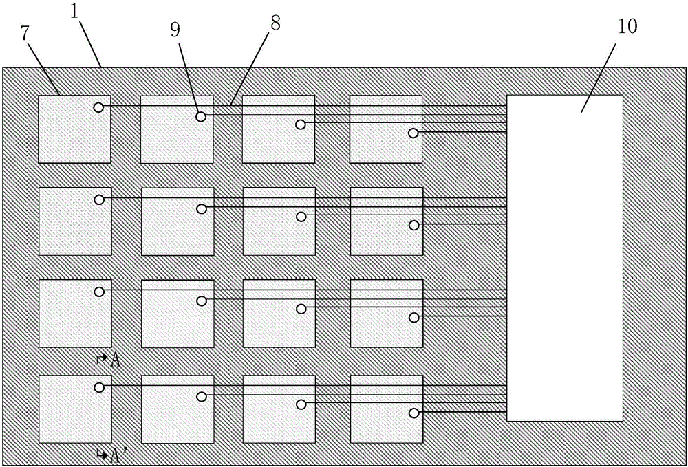
[0041] figure 1 A top view of the gene sequencing chip of Example 1 is shown. figure 2 It is the edge of the gene sequencing chip of embodiment 1 figure 1 A cross-sectional view taken along line A-A'.

[0042] Such as figure 1 As shown, the gene sequencing chip includes a substrate 1, on which an electrode 7 and a signal lead 8 are arranged, one end of the signal lead 8 is connected to the electrode 7, and the other end is connected to a detection chip 10 as a signal sending end, and the detection chip 10 is set On one or both sides of the array composed of sequencing units, the detection chip 10 sends a voltage pulse signal to the electrode 7 through the signal lead 8, and detects whether the signal value sensed by the electrode 7 changes. exist figure 1 Among them, the electrodes 7 and the signal leads 8 are arranged in different layers, and are connected through the via holes 9 on the third insulating layer 4 . The electrodes 7 and the signal leads 8 are made of m...

Embodiment 2

[0058] The difference between the gene sequencing chip of this embodiment and the gene sequencing chip in Example 1 will be mainly described below, and the description of the same parts will be omitted for the sake of brevity, wherein the same reference numerals represent the same components.

[0059] Figure 5 A top view of the gene sequencing chip of Example 2 is shown. Figure 6 It is the edge of the gene sequencing chip of embodiment 2 Figure 5 A cross-sectional view taken along line A-A'.

[0060] Such as Figure 5 As shown, the signal leads 8 and the electrodes 7 are arranged on the same layer. Such as Figure 6 As shown, the electrodes 7 are directly formed on the substrate 1 and connected to the signal leads 8 on the same layer.

[0061] Of course, the arrangement of the first insulating layer 2 and the second insulating layer 3 is not limited to the arrangement in the first embodiment.

[0062] For example, Figure 7 Is according to embodiment 2 a modified emb...


PUM


Abstract

The invention provides a gene sequencing chip, a gene sequencing apparatus and a gene sequencing method. The gene sequencing chip comprises a substrate (1), an electrode (7), a signal lead (8) and a first insulation layer (2), wherein the electrode (7) is formed on the substrate (1); the signal lead (8) is connected with the electrode (7) and is used for sending a signal to the electrode (7) and outputting the signal sensed by the electrode (7) to a signal sending end; the first insulation layer (2) is arranged on the substrate (1) with the formed electrode (7) and signal lead (8); a micropore (5) is formed in a position on the first insulation layer (2) corresponding to the electrode (7) and is arranged at one side of the electrode (7) away from the substrate (1); and the micropore (5) and the electrode (7) are separated by a second insulation layer (3).The gene sequencing chip in the invention needs no field effect tube, is simple in manufacturing process and can greatly lower the manufacturing difficulty and cost.

Description

technical field [0001] The invention relates to the field of gene sequencing, in particular to a gene sequencing chip, gene sequencing equipment and a gene sequencing method. Background technique [0002] Gene sequencing technology is the most commonly used technology in modern molecular biology research. Since the development of the first generation of gene sequencing in 1977, gene sequencing technology has achieved considerable development, mainly including the first generation of Sanger sequencing technology, the second generation of Qualcomm Quantitative sequencing technology, third-generation single-molecule sequencing technology and fourth-generation nanopore sequencing technology. At present, the mainstream sequencing technology in the market is still dominated by second-generation high-throughput sequencing. [0003] The second-generation high-throughput sequencing technologies mainly include Illumina's sequencing-by-synthesis technology, Thermo Fisher's ion semicon...

Claims


Application Information

Patent Timeline
IPC IPC(8): C12M1/34C12Q1/68
CPCC12Q1/6869C12Q2565/607C12Q2535/122C12Q2565/631C12Q1/6874G01N33/48721C12Q2535/101C12Q2563/116G01N27/333G01N27/3276
Inventor 庞凤春蔡佩芝耿越
Owner BOE TECH GRP CO LTD
Features
  • R&D
  • Intellectual Property
  • Life Sciences
  • Materials
  • Tech Scout
  • Unparalleled Data Quality
  • Higher Quality Content
  • 60% Fewer Hallucinations
Learn More