An endpoint monitoring method for backhole etching of high electron mobility transistors

A technology with high electron mobility and transistors, which is applied in the testing/measurement of circuits, electrical components, semiconductors/solid-state devices, etc., can solve the problems of weak signal of the endpoint monitoring system, small proportion of exposed area of ​​back holes, and difficult identification, etc., to achieve High practical value, improved process reliability, improved accuracy and effectiveness

Active Publication Date: 2019-03-26
CHENGDU HIWAFER SEMICON CO LTD
View PDF4 Cites 0 Cited by
  • Summary
  • Abstract
  • Description
  • Claims
  • Application Information

AI Technical Summary

Problems solved by technology

However, the characteristic spectroscopy method has the following disadvantages: the exposed area of ​​the back hole is relatively small, resulting in a weak signal of the endpoint monitoring system and difficult to identify

Method used


Image

  • An endpoint monitoring method for backhole etching of high electron mobility transistors
  • An endpoint monitoring method for backhole etching of high electron mobility transistors
  • An endpoint monitoring method for backhole etching of high electron mobility transistors

Examples


Embodiment Construction

[0018] In order to make the purpose, technical solution and advantages of the present application clearer, the present application will be further described in detail below in conjunction with the accompanying drawings and specific embodiments. For simplicity, some technical features known to those skilled in the art are omitted from the following description.

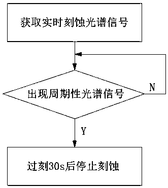
[0019] In this embodiment, a silicon carbide-based gallium nitride high electron mobility transistor is taken as an example. The complete process of back hole etching and endpoint monitoring is as follows:

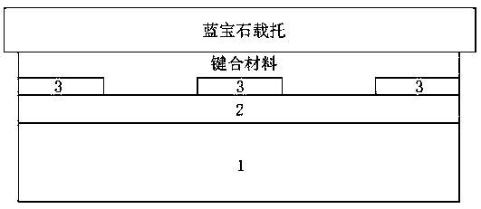
[0020] A. Two kinds of metals are grown alternately on the wiring layer of the device front process to form a periodic metal layer 3, and the periodic metal layer 3 is located above the position of the through hole to be etched on the back, such as figure 2 Shown; Alternately grown metals are platinum and gold, or nickel and gold, that is, a periodic structure of Pt / Au / Pt / Au / Pt / Au or Ni / Au / Ni / Au / Ni / Au, typical thi...


PUM


Abstract

The invention provides a terminal point monitoring method of high-electron-mobility transistor back hole etching. Two kinds of metal are alternatively grown on a wiring layer of a device right side technology so as to form a periodic metal layer. The periodic metal layer is located above a position of a back side through hole to be etched. The terminal point monitoring method comprises the following steps of S1, acquiring a real-time etching spectrum signal; S2, determining whether to generate a periodic spectrum signal; S3, if the periodic spectrum signal is generated, stopping etching after 30s over etching; and S4, if the periodic spectrum signal is not generated, repeatedly executing the step S2. In the invention, through a periodic lamination design wiring a periodic metal layer in a right side, an identification degree and sensitivity of a terminal point signal of a terminal point monitoring system are increased and accuracy and validity of terminal point decision are increased too; the method is especially suitable for silicon-carbide-based gallium nitride high-electron-mobility transistor back hole etching with an exposed area proportion which is not high (<2%); and technology reliability of back hole etching can be obviously improved and a high practical value is possessed.

Description

technical field [0001] The invention relates to the technical field of semiconductors, in particular to an endpoint monitoring method for back hole etching of high electron mobility transistors. Background technique [0002] GaN-based high electron mobility transistor (HEMT) has become the technology of choice for next-generation RF / microwave power amplifiers due to its unique high electron mobility, high two-dimensional electron gas surface density, and high breakdown electric field. [0003] The GaN HMET process is divided into front-side process and back-side process. The back-side process mainly completes wafer thinning and back-hole interconnection. Among them, the back-hole process is particularly important, and it is the interconnection path between the front device and the back metal ground plane. The quality of the back-hole process directly determines the quality of the product. [0004] At present, GaN HEMT back hole processing technology is mainly composed of Si...

Claims


Application Information

Patent Timeline
Patent Type & Authority Patents(China)
IPC IPC(8): H01L21/66
CPCH01L22/26
Inventor 孔欣
Owner CHENGDU HIWAFER SEMICON CO LTD
Why Eureka
Try Eureka