Chip encapsulation structure, manufacture method thereof and electrostatic powder spraying device

A technology of chip packaging structure and electrostatic powder, which is applied in the direction of electrostatic spraying device, spraying device, spray discharge device, etc., can solve the problem of chip function failure, etc., and achieve the effect of improving quality, good thermal stability and easy implementation

Active Publication Date: 2017-03-15
SEMICON MFG INT TIANJIN +1
View PDF4 Cites 5 Cited by
  • Summary
  • Abstract
  • Description
  • Claims
  • Application Information

AI Technical Summary

Problems solved by technology

[0010] The purpose of the present invention is to provide a chip packaging structure and its manufacturing method, and an electrostatic powder spraying device to solve the problem of chip function failure caused by silver glue overflowing and covering the upper surface of the chip in the existing chip bonding process

Method used


Image

  • Chip encapsulation structure, manufacture method thereof and electrostatic powder spraying device
  • Chip encapsulation structure, manufacture method thereof and electrostatic powder spraying device
  • Chip encapsulation structure, manufacture method thereof and electrostatic powder spraying device

Examples


Embodiment 1

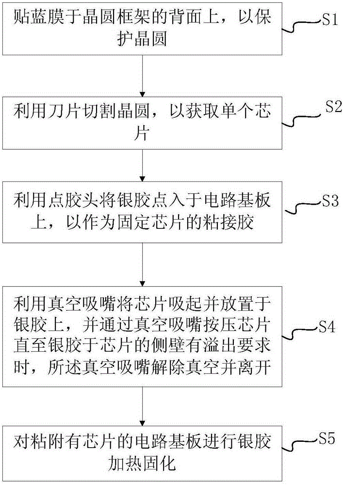
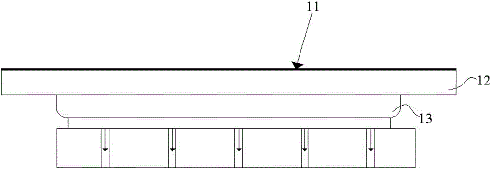
[0051] refer to Figure 10with Figure 11 , the chip packaging structure of this embodiment includes a circuit substrate 21, an adhesive layer 22 disposed on the circuit substrate 21, and a chip 23 disposed on the adhesive layer 22, wherein the sidewall of the chip 23 is provided with Layer 24 of non-stick material.

[0052] The bonding adhesive layer 22 is a conductive adhesive layer, such as conductive silver adhesive. The components of the conductive silver glue include epoxy resin, acid anhydride curing agent and modified imidazole compound accelerator.

[0053] The non-stick material layer 24 is preferably made of polytetrafluoroethylene (PTFE). Of course, the present invention includes but is not limited to polytetrafluoroethylene materials, and other non-stick materials can also be used as long as they have properties similar to polytetrafluoroethylene materials.

[0054] Using polytetrafluoroethylene material, on the one hand, it has excellent heat resistance chara...

Embodiment 2

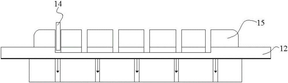
[0074] This embodiment provides an electrostatic powder spraying device, which is used for spraying electrostatic powder on the sidewall of the chip during the chip packaging process to form a non-stick material layer. The use of electrostatic spraying can not only save paint, improve chip packaging efficiency, but also save labor costs.

[0075] Such as Figure 14 As shown, the electrostatic powder spraying device of this embodiment includes a powder supply unit 30 and a spray unit 40 connected to the powder supply unit 30, wherein the powder supply unit 30 is used to provide powder 31, and the spray unit 40 is used to spray powder 31 and make the powder 31 atomized or atomized more uniformly, and then electrostatically adsorbed on the sidewall of the chip 51 to be sprayed. Here, the atomization means that the particles in the powder contain the same charge, so that the powders repel each other on the transmission path, thereby forming a uniform cloud-like spray, and the spr...


PUM


Abstract

The present invention provides a chip encapsulation structure, a manufacture method thereof and an electrostatic powder spraying device. The chip encapsulation structure includes a circuit substrate, an adhesive layer arranged on the circuit substrate, and a chip arranged on the adhesive layer; and the side wall of the chip is provided with a non-stick material layer. The manufacture method of the chip encapsulation structure includes the following steps that: a chip for encapsulation is provided; a non-stick material layer is arranged on the side wall of the chip; a circuit substrate for carrying the chip is provided; an adhesive layer is arranged on the circuit substrate; the chip is arranged on the adhesive layer, and the bottom of the chip is completely covered with the adhesive layer; and the adhesive layer is heated, so that the adhesive layer can be cured. According to the chip encapsulation structure, the manufacture method thereof and the electrostatic powder spraying device of the invention, the non-stick material layer is arranged on the side wall of the chip, so that the overflowed adhesive layer will not adhere to the upper surface of the chip, and therefore, the malfunctioning of the chip can be avoided, the reliability of the chip can be ensured, and the quality of the chip encapsulation structure can be improved.

Description

technical field [0001] The invention relates to semiconductor chip packaging technology, in particular to a chip packaging structure, a manufacturing method thereof, and an electrostatic powder spraying device. Background technique [0002] In semiconductor technology, silicon, quartz, lithium niobate, lithium tantalate and other materials are generally used for the production of the substrate. After cleaning, coating, photolithography and other processes, the substrate is made to contain multiple chips with complete electrical properties. The substrate, and then through the packaging process to achieve product molding. The packaging process directly determines the reliability of the product, which usually includes steps such as blue film pasting, substrate cutting and slicing, and chip bonding. [0003] Existing chip packaging processes such as Figure 1-9 shown, including: [0004] Step S1: Paste the blue film 11 on the back of the wafer frame 12 to protect the wafer 13,...

Claims


Application Information

Patent Timeline
Patent Type & Authority Applications(China)
IPC IPC(8): H01L23/29H01L23/31H01L21/56B05B5/00B05B5/025
Inventor 牛刚
Owner SEMICON MFG INT TIANJIN
Why Eureka
Try Eureka