Supercharge Your Innovation With Domain-Expert AI Agents!

Bootstrap diode structure based on P-type substrate and manufacturing process

A diode and substrate technology, applied in the field of semiconductor device structure and its manufacturing process, can solve the problems of increasing peripheral circuit connection, destroying circuit timing, increasing chip cost, etc., and achieving improved reliability, low cost and process difficulty, and low cost Effect

Inactive Publication Date: 2017-04-19
南京星焱微电子科技有限公司
View PDF1 Cites 0 Cited by
  • Summary
  • Abstract
  • Description
  • Claims
  • Application Information

AI Technical Summary

Problems solved by technology

[0005] The use of external bootstrap diodes needs to increase the connection of peripheral circuits, which reduces the reliability and increases the overall cost;
[0006] If the diode is directly integrated on the bulk silicon material, due to the reverse recovery characteristics of the diode, there will be a large number of minority carriers (minority carriers) in the reverse direction, which will generate a minority carrier current and destroy the circuit timing; so it is necessary to use SOI (Silicon On Insulator Silicon-on-insulator structure) process isolation can directly integrate diodes, but in this case, the process is complicated and the cost is high;
[0007] A chip with a bootstrap diode structure that uses an integrated Charge Pump+integrated high-voltage MOSFET structure requires a special MOSFET process, such as a thick gate oxide process (double gate oxide process), and the production of a Charge Pump requires a large chip area, increasing the number of chips cost

Method used


Image

  • Bootstrap diode structure based on P-type substrate and manufacturing process
  • Bootstrap diode structure based on P-type substrate and manufacturing process
  • Bootstrap diode structure based on P-type substrate and manufacturing process

Examples


Embodiment Construction

[0020] The present invention will be further described below in conjunction with accompanying drawing:

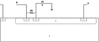
[0021] Such as image 3 As shown, the integrated circuit structure of the present invention includes a P-type lightly doped substrate 1; an N well region 2; 3 and 5 are N+ regions; 4 and 6 are P+ regions. 4 and 5 are connected through resistor R1, and 4 is connected with GND through switch S1. The switch of S1 is realized by the control signal; 6 is generally connected to the ground or the common terminal; 5, 4, 3, and 2 form a JFET, 5 is the drain terminal, 2 is the channel, 4 is the gate, and 3 is the source terminal ;

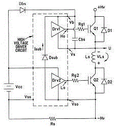
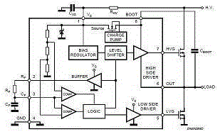
[0022] This structure is equivalent to a bootstrap diode and can replace figure 1 The function of Dbs in Dbs, where the D terminal (5) is connected to the positive pole of Vcc, and the S terminal (3) is connected to the upper plate of Vb and Cbs; it can also replace figure 2 The charge pump in and the connected MOSFET;

[0023] Realization function ...


PUM


Abstract

The invention discloses an integrated circuit structure which comprises an electronic switch, a resistor module and a semiconductor structure on the P-type substrate, wherein the semiconductor structure has a junction type field effect transistor arranged therein. Turning on / off of the junction type field effect transistor in the semiconductor structure is controlled by the electronic switch and other parts of the semiconductor structure, thereby realizing same function with a bootstrap diode in a grid driving circuit. The invention further discloses a manufacturing process of the integrated circuit structure. The process can be simply integrated in a chip process without increasing extra process steps, and production is easy.

Description

technical field [0001] The invention relates to an integrated circuit structure and a manufacturing process thereof, in particular to a semiconductor device structure based on a P-type substrate and having the same function as a bootstrap diode and a manufacturing process thereof. Background technique [0002] Such as figure 1 When the MOS tube of the half-bridge is driven, it is generally the timing sequence that the upper tube and the lower tube are turned on in turn; when the upper tube is turned off and the lower tube is turned on, the potential of Vs is the common terminal potential (generally 0), The potential of the drain (Drain terminal) of Q1 is HV (such as 600V). At this time, Vcc is charged to Cbs through Dbs. After being fully charged, Cbs provides a driving voltage Vg1=Vcc (such as 20V) for the upper tube driver (Drv1). The control terminal signal Control the switch of Q1; when the upper tube is turned on and the lower tube is turned off, the potential of the V...

Claims


Application Information

Patent Timeline
IPC IPC(8): H01L27/06H01L21/8249
CPCH01L27/0629H01L21/8249
Inventor 胡浩宁小霖
Owner 南京星焱微电子科技有限公司
Features
  • R&D
  • Intellectual Property
  • Life Sciences
  • Materials
  • Tech Scout
  • Unparalleled Data Quality
  • Higher Quality Content
  • 60% Fewer Hallucinations
Learn More