Liquid crystal display panel and method of manufacturing and restoring the same

A liquid crystal display panel and repair method technology, applied in nonlinear optics, instruments, optics, etc., can solve the problems of easy distortion of display images, large liquid crystal display panel space, signal distortion, etc.

Inactive Publication Date: 2017-04-26
NANJING CEC PANDA LCD TECH
View PDF6 Cites 5 Cited by
  • Summary
  • Abstract
  • Description
  • Claims
  • Application Information

AI Technical Summary

Problems solved by technology

[0003] Since the vertical common electrode 3 is formed before the JAS hole 6, it is inevitable that there is a certain gap 8 between the vertical common electrode 3 and the pixel electrode 7, which seriously limits the aperture ratio of the pixel electrode; in addition, the impedance of the J

Method used


Image

  • Liquid crystal display panel and method of manufacturing and restoring the same
  • Liquid crystal display panel and method of manufacturing and restoring the same
  • Liquid crystal display panel and method of manufacturing and restoring the same

Examples


Embodiment Construction

[0034] Below in conjunction with accompanying drawing and specific embodiment, further illustrate the present invention, should be understood that these embodiments are only for illustrating the present invention and are not intended to limit the scope of the present invention, after having read the present invention, those skilled in the art will understand various aspects of the present invention Modifications in equivalent forms all fall within the scope defined by the appended claims of this application.

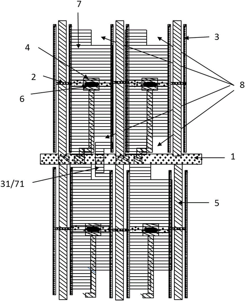
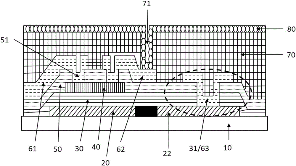
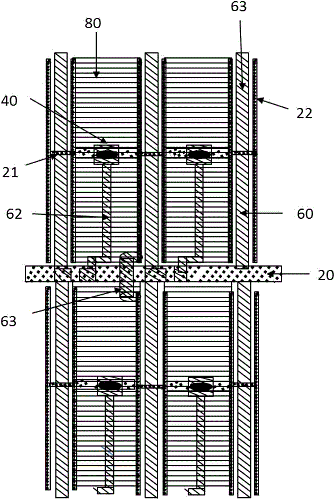
[0035] Such as figure 2 and image 3 Shown is a schematic diagram of the structure of an IGZO liquid crystal display panel. IGZO is an abbreviation of a metal oxide, namely: (indium gallium zinc oxide) is an abbreviation of indium gallium zinc oxide, wherein the atomic ratio of indium gallium zinc oxide is: 1 :1:1:4.

[0036] The manufacturing steps of IGZO's liquid crystal display panels are:

[0037] The first step: on the glass substrate 10, the gate 20 formed by ...


PUM


Abstract

The invention provides a liquid crystal display panel and a method of manufacturing and restoring the same. The liquid crystal display panel comprises vertically and horizontally staggered grids and data lines, a horizontal common electrode line, a grating insulating layer on the grating, a metal-oxide semiconductor layer on the grating insulating layer, an etching barrier layer on the metal-oxide semiconductor layer, a source electrode, a drain electrode, a JAS layer, a second metal connecting line which is connected with a longitudinal common electrode, and a pixel electrode, wherein the horizontal common electrode line and the grading are formed at the same time; the source electrode and the drain electrode are electrically connected with the metal-oxide semiconductor layer; and the JAS layer covers the source electrode, the drain electrode, the second metal connecting line and a data line. The liquid crystal display panel and the method of manufacturing and restoring the same can solve the problem that a current pixel is small in the aperture ratio and is distorted, thus reducing the time of signal transmission, avoiding distortion caused by signal delay, and at the same time can reduce the line layout surrounding a panel and save the space of the panel and the production cost.

Description

technical field [0001] The invention relates to the technical field of liquid crystal display, in particular to a liquid crystal display panel and its manufacturing and repairing methods. Background technique [0002] Existing liquid crystal display panels that use amorphous silicon as the semiconductor layer, such as figure 1 As shown, the design of the amorphous silicon liquid crystal display panel mainly considers the bridging of the upper and lower pixels. The manufacturing steps of the amorphous silicon liquid crystal display panel are: the first step: the pattern of the gate 1 formed by the first metal, The pattern of the horizontal common electrode 2 parallel to the gate 1 and the vertical and horizontal common electrode 3 parallel to the predetermined data line 5; the second step: forming a gate insulating layer (not shown) covering the first metal layer; the third step: Forming a semiconductor layer 4 made of amorphous silicon; the fourth step: forming the source a...

Claims


Application Information

Patent Timeline
IPC IPC(8): G02F1/13G02F1/1362
CPCG02F1/1309G02F1/136259G02F1/136263
Inventor 刘文雄田汝强
Owner NANJING CEC PANDA LCD TECH
Why Eureka
Try Eureka