
A high-speed image exposure method for dmd maskless lithography machine

A technology of maskless lithography and high-speed imaging, which is applied in microlithography exposure equipment, photomechanical equipment, and photolithography process exposure equipment, etc., can solve the problems of large data volume and limit the working efficiency of lithography machines, and achieve high-speed Effects of data transmission, improving DMD image exposure speed, and optimizing exposure control process

Inactive Publication Date: 2018-03-09
UNIV OF ELECTRONICS SCI & TECH OF CHINA
View PDF10 Cites 2 Cited by
  • Summary
  • Abstract
  • Description
  • Claims
  • Application Information

AI Technical Summary

Problems solved by technology

However, in the scanning exposure process, for each scanning step, the DMD needs to scroll to refresh an exposure image, so that the data volume of the DMD exposure image is very large, and it will be serious to transmit all the real-time exposure images of the DMD through the communication interface. Limit the work efficiency of the lithography machine

Method used


Image

  • A high-speed image exposure method for dmd maskless lithography machine
  • A high-speed image exposure method for dmd maskless lithography machine
  • A high-speed image exposure method for dmd maskless lithography machine

Examples


Embodiment

[0024] For the convenience of description, the relevant technical terms appearing in the specific implementation are explained first:

[0025] DMD (Digital Micromirror Device): digital micromirror device;

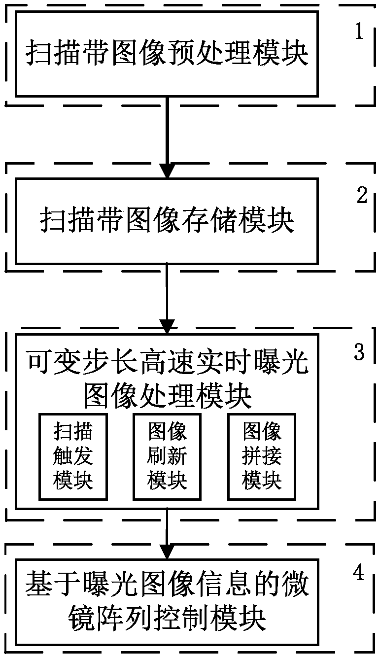
[0026] figure 1 It is a system block diagram of a high-speed image exposure method for a DMD maskless lithography machine.

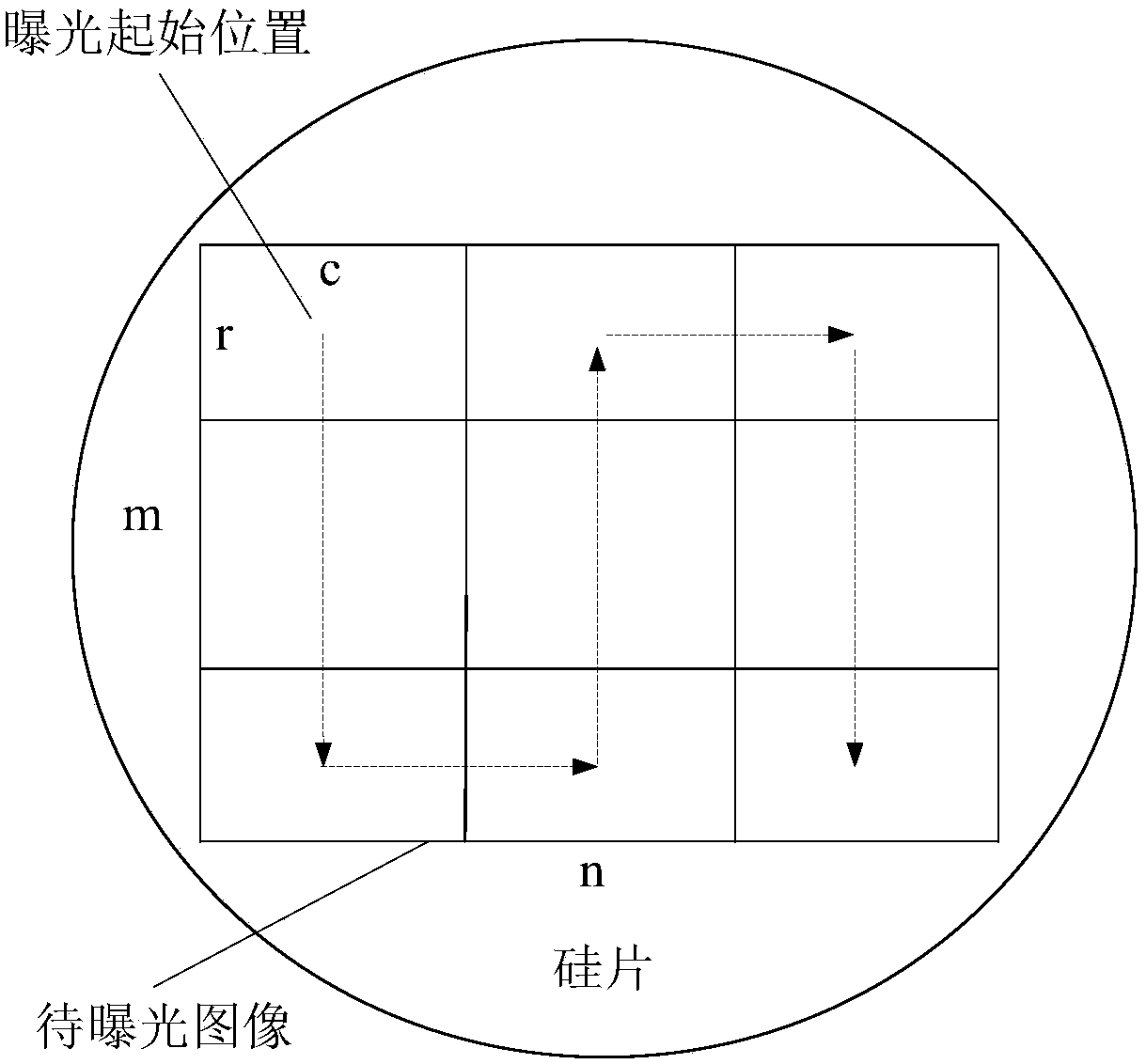
[0027] In this embodiment, the core controller of the control board of the DMD takes Xilinx Virtex-5 type FPGA as an example, and the storage device takes DDR2 as an example, and the original image to be exposed is a bitmap image with a resolution of 10000×10000 As an example, DMD takes the 0.7XGA model as an example, and its resolution is 768×1024. It can be understood that the application of other types of controllers, storage devices, and DMDs is naturally also included in the protection scope of the present invention.

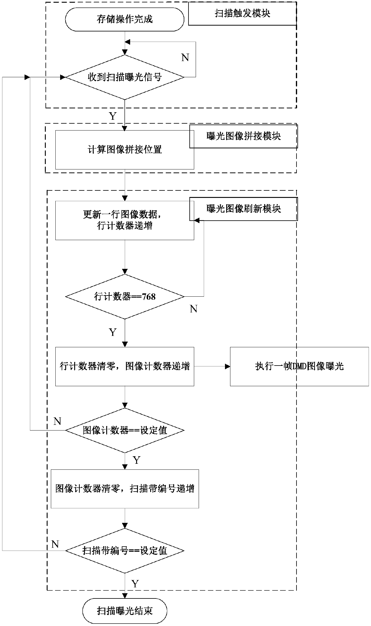
[0028] Combined below as figure 1 As shown, a high-speed image exposure method for a DMD maskless photolithography machine of...


PUM


Abstract

The invention discloses a high-speed image exposure method for a DMD maskless lithography machine, optimizes the DMD lithography exposure control process, avoids directly sending real-time exposure images to the DMD for exposure by the host computer software, and uses a storage device instead The image to be processed is cached, and the high-speed real-time exposure image processing is completed through the DMD control board instead of the host computer software, without the need for a communication interface transmission for each frame of the DMD real-time exposure image, reducing the amount of transmitted data and effectively reducing the transmission of the communication interface The speed limits the lithography efficiency. In the actual exposure stage, the exposure image information is directly obtained from the external storage device, and based on the exposure image information, the DMD micromirror array is automatically controlled to complete the rapid flip, giving full play to the high-speed data transmission and the hardware control board. The advantage of powerful timing control ability greatly shortens the data transmission time, improves the DMD image exposure speed, and improves the working efficiency of the DMD maskless lithography machine.

Description

technical field [0001] The invention belongs to the technical field of maskless lithography, and more specifically relates to a high-speed image exposure method for a DMD maskless lithography machine. Background technique [0002] In traditional projection lithography, the fabrication and processing of the photomask used in the exposure process is a relatively cumbersome and complicated process, which also has high requirements on the mask and lithography process, and the processing cost is relatively expensive. To solve this problem, a digital maskless lithography technology based on digital micromirror device (DMD) has been gradually applied. DMD-based maskless lithography technology can use ultraviolet light, deep ultraviolet light, and even shorter-wavelength extreme ultraviolet light as light sources. It has strong technical extension and process compatibility, and meets the requirements of flexibility, high efficiency, and low cost. , is easier to be applied in lithog...

Claims


Application Information

Patent Timeline
Patent Type & Authority Patents(China)
IPC IPC(8): G03F7/20
CPCG03F7/70383G03F7/70508
Inventor 邹见效彭超池文明徐红兵何健
Owner UNIV OF ELECTRONICS SCI & TECH OF CHINA
Learn More