Packaging technology and packaging structure of ceramic chip

A technology of chip packaging structure and packaging technology, which is applied in the manufacture of electrical components, electrical solid devices, semiconductor/solid devices, etc., can solve the problems of contaminating the connection area of ​​ceramic chips, reducing labor and transportation costs, etc., and achieve product yield improvement, The effect of reducing labor and transportation costs and convenient operation

Inactive Publication Date: 2017-05-10
NANJING NUOBANG NEW MATERIAL CO LTD
View PDF4 Cites 2 Cited by
  • Summary
  • Abstract
  • Description
  • Claims
  • Application Information

AI Technical Summary

Problems solved by technology

[0005] The technical problems to be solved by the present invention are: (1) How to prevent the traditional liquid glue from polluting the connection area between the ceramic chip and the lead wire in the cover plate sealing process; The airtightness of the chip; (3) How to make the ceramic chip packaging process easy to operate, greatly reducing labor and transportation costs

Method used


Image

  • Packaging technology and packaging structure of ceramic chip
  • Packaging technology and packaging structure of ceramic chip
  • Packaging technology and packaging structure of ceramic chip

Examples


Embodiment 1

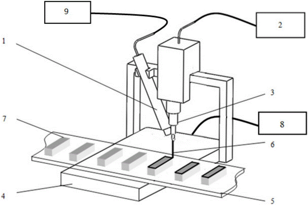
[0032] This embodiment is a packaging process for ceramic chips, such as figure 1 shown, including the following steps:

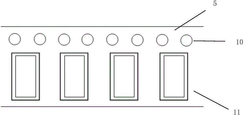
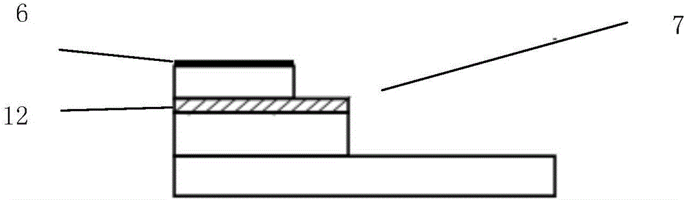
[0033] (1) Dispensing and film formation: Before chip assembly, apply liquid dual-cure sealant to the outer edge of the side of the ceramic carrier that needs to be packaged with the cover plate through a dispenser, and cure the dual-cure sealant by UV light irradiation Shaped to form a structural adhesive film on the ceramic carrier; the dispenser includes a horizontal moving platform 4 whose displacement and direction are controlled by the first controller 8, a dispensing head 3 whose glue output is controlled by the second controller 2, and a horizontal moving platform 4 The displacement and direction are controlled by the first controller 8; the glue output of the dispensing head 3 is controlled by the second controller 2; the glue is applied to the outer edge 7 of the ceramic carrier through the dispensing head 3 to form a horizontal glue line 6, and t...


PUM

PropertyMeasurementUnit
thicknessaaaaaaaaaa
thicknessaaaaaaaaaa

Abstract

The invention provides a packaging technology of a ceramic chip. The packaging technology comprises the following steps of (I) dispensing and film-forming, before chip assembly, coating the edge of one side, which needs to be packaged with a cover plate, of a ceramic carrier with a liquid-like dual-curable sealant through a glue dispenser, and curing and setting the dual-curable sealant through UV light irradiation to form a structural film on the ceramic carrier; (2) chip assembly, namely carrying out chip assembly on the ceramic carrier; and (3) cured sealing, after chip assembly is completed, bonding the cover plate matched with the ceramic carrier in size and the ceramic carrier through heating the structural film and then carrying out cured sealing. The packaging structure of the ceramic chip has the practical advantages of high bonding strength, good surface wettability, high air-tightness and the like, the roll-to-roll automatic dispensing process can be achieved and the production efficiency is obviously improved.

Description

technical field [0001] The invention relates to the technical field of ceramic chip packaging, and relates to a ceramic chip packaging process and a packaging structure thereof. Background technique [0002] Ceramic materials are heterogeneous inorganic non-metallic materials made of natural or synthetic compounds after forming and high-temperature firing. In terms of thermal and mechanical properties, they have the advantages of high temperature resistance, heat insulation, high hardness, and wear resistance; Insulation, piezoelectricity, semiconductivity, magnetism, etc.; chemically, it has functions such as catalysis, corrosion resistance, and adsorption. [0003] Ceramic packaging is a new type of packaging method developed after metal packaging. Like metal, it is also airtight. The ceramic shell (carrier) is made of multi-layer ceramic microwave technology, through ceramic powder, casting, blanking, Punching, printing, lamination, hot cutting, sintering, nickel plating...

Claims


Application Information

Patent Timeline
Patent Type & Authority Applications(China)
IPC IPC(8): H01L21/56H01L23/31H01L23/29
CPCH01L21/56H01L23/291H01L23/3114H01L21/60H01L2224/48091H01L2924/00014
Inventor 刘兵张奥涵刘勇
Owner NANJING NUOBANG NEW MATERIAL CO LTD
Why Eureka
Try Eureka