OLED (Organic Light Emitting Diode) encapsulation method and OLED encapsulation structure

An encapsulation method and encapsulation structure technology, applied in the structure of organic light-emitting devices, gaseous chemical plating, coating, etc., can solve the problems of low light penetration, easy cracks, large film stress, etc., and achieve high thermal conductivity , Improve performance and service life, good flexibility effect

Active Publication Date: 2017-05-10
WUHAN CHINA STAR OPTOELECTRONICS TECH CO LTD
View PDF8 Cites 13 Cited by
  • Summary
  • Abstract
  • Description
  • Claims
  • Application Information

AI Technical Summary

Problems solved by technology

However, due to the high density of the pure DLC film, the light penetration is not high, and the stress of the film is large, which is prone to cracks when bent

Method used


Image

  • OLED (Organic Light Emitting Diode) encapsulation method and OLED encapsulation structure
  • OLED (Organic Light Emitting Diode) encapsulation method and OLED encapsulation structure
  • OLED (Organic Light Emitting Diode) encapsulation method and OLED encapsulation structure

Examples


no. 1 example

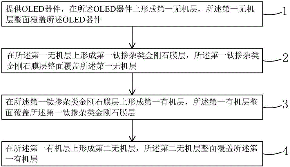
[0044] see figure 1 , is the first embodiment of the OLED packaging method of the present invention, which includes the following steps:

[0045] Step 1, such as figure 2 and image 3 As shown, an OLED device 101 is provided, and a first inorganic layer 201 is formed on the OLED device 101 , and the first inorganic layer 201 covers the entire surface of the OLED device 101 .

[0046] Specifically, in step 1, plasma enhanced chemical vapor deposition (Plasma Enhanced Chemical Vapor Deposition, PECVD), atomic layer deposition (Atomic Layer Deposition, ALD), pulsed laser deposition (Pulsed Laser Deposition, PLD), or sputtering (Sputter) method to form the first inorganic layer 201 .

[0047] Specifically, the material of the first inorganic layer 201 includes aluminum oxide (Al 2 o 3 ), titanium dioxide (TiO 2 ), silicon nitride (SiN x ), silicon carbonitride (SiCN x ), and silicon oxide (SiO x ) in one or more.

[0048] Specifically, the thickness of the first inorgan...


PUM

PropertyMeasurementUnit
thicknessaaaaaaaaaa
thicknessaaaaaaaaaa
thicknessaaaaaaaaaa

Abstract

The invention provides an OLED (Organic Light Emitting Diode) encapsulation method and an OLED encapsulation structure. A titanium-doped diamond film layer is introduced into an OLED film encapsulation layer; the light transmittance, bending property, thermal conductivity and water-oxygen blocking capability of the OLED film encapsulation layer are improved by using relatively high light transmittance, relatively good flexibility, high thermal conductivity and relatively low water-oxygen transmittance of the titanium-doped diamond film layer, and then the usability and service life of an OLED display panel are improved.

Description

technical field [0001] The invention relates to the field of display technology, in particular to an OLED packaging method and an OLED packaging structure. Background technique [0002] Organic Light Emitting Display (OLED) has self-illumination, low driving voltage, high luminous efficiency, short response time, high definition and contrast, nearly 180° viewing angle, wide operating temperature range, and can realize flexible display and With many advantages such as large-area full-color display, it is recognized by the industry as a display device with the most potential for development. [0003] According to the driving method, OLED can be divided into two categories: passive matrix OLED (Passive Matrix OLED, PMOLED) and active matrix OLED (Active Matrix OLED, AMOLED), namely direct addressing and thin film transistor matrix addressing. Among them, AMOLED has pixels arranged in an array, belongs to the active display type, has high luminous efficiency, and is usually use...

Claims


Application Information

Patent Timeline
Patent Type & Authority Applications(China)
IPC IPC(8): H01L51/52H01L51/56
CPCH10K71/00H10K2102/302H10K71/16H10K50/8445C23C16/26H10K2102/311
Inventor 彭斯敏金江江
Owner WUHAN CHINA STAR OPTOELECTRONICS TECH CO LTD
Why Eureka
Try Eureka