Method for final polishing of silicon wafer, and silicon wafer polished by method
一种精抛光、硅晶圆的技术,应用在含研磨剂的抛光组合物、化学仪器和方法、磨削/抛光设备等方向,能够解决增加晶圆微小表面缺陷、易凝结、过滤困难等问题,达到雾度等级优良、雾度不均少、微小缺陷少的效果
- Summary
- Abstract
- Description
- Claims
- Application Information
AI Technical Summary
Problems solved by technology
Method used
Image
Examples
Embodiment
[0053] Hereinafter, the present invention will be more specifically described by showing examples and comparative examples of the present invention, but the present invention is not limited to these examples and comparative examples.
[0054]
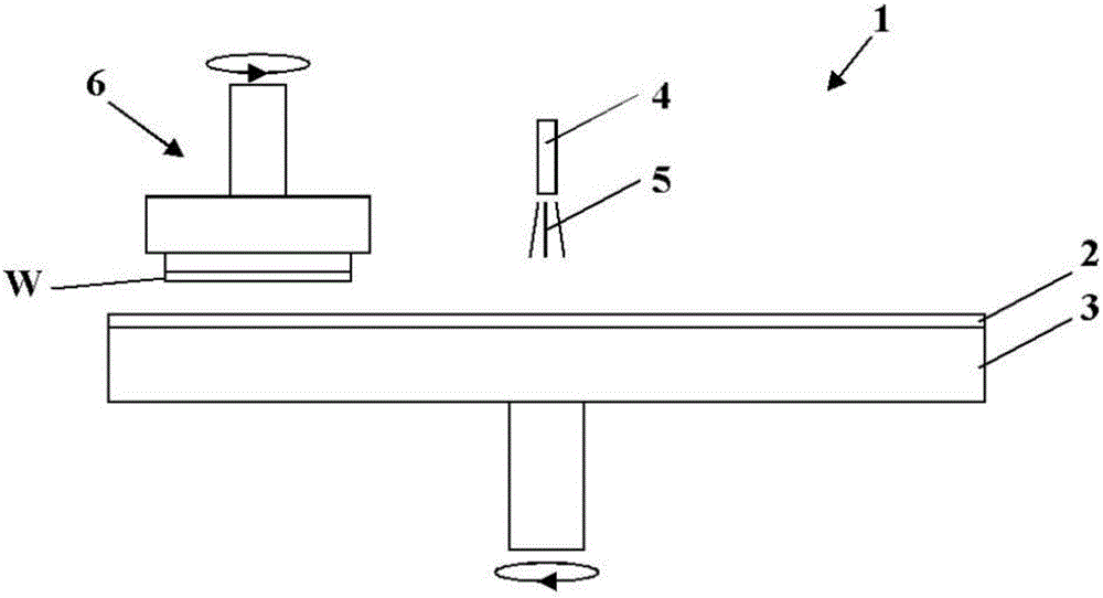
[0055] The fine polishing of the silicon wafer is completed by the fine polishing method of the present invention.
[0056] First, abrasive grains (silica gel with an average primary particle size of 25 nm measured by BET method), ammonia, hydroxyethyl cellulose and pure water were mixed to prepare a polishing agent. In Example 1, the weight average molecular weight of hydroxyethyl cellulose was 500,000. In addition, the weight average molecular weight of hydroxyethyl cellulose was computed as the polyethylene oxide conversion value using the cycle gel permeation chromatography. In addition, at this time D 1 / D 2 The value of 1.86.
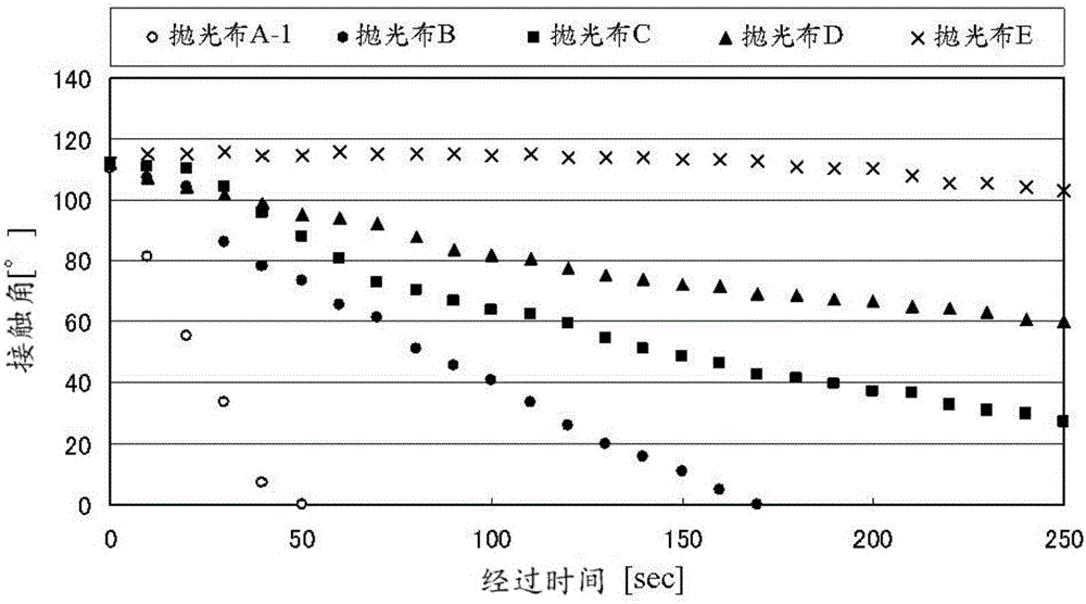
[0057] The polishing cloth is used as shown in Figure 5 The polishing cloth E. The polishing cl...
Embodiment 2
[0065] In addition to changing the weight average molecular weight of hydroxyethyl cellulose in the polishing agent to 400,000, and changing D 1 / D 2 Except changing to 1.51, the silicon wafer was polished under the same conditions as in Example 1, and the quality of the polished wafer was evaluated.
[0066] As a result, it can be seen from Table 1 that, while the haze level was good, the haze unevenness (Defect%) was a good value of 3.3%, which was lower than the pass standard of 5.0%. In addition, satisfactory results were also obtained with respect to minute defects.
Embodiment 3
[0068] In addition to changing the weight average molecular weight of hydroxyethyl cellulose in the polishing agent to 700,000, and changing D 1 / D 2 Except changing to 2.28, the silicon wafer was polished under the same conditions as in Example 1, and the quality of the polished wafer was evaluated.
[0069] As a result, as can be seen from Table 1, while the haze level was good, the haze unevenness (Defect %) was a good value of 2.9%, which was lower than the pass standard of 5.0%. In addition, satisfactory results were also obtained with respect to minute defects.
PUM
| Property | Measurement | Unit |
|---|---|---|
| particle diameter | aaaaa | aaaaa |
| water contact angle | aaaaa | aaaaa |
| particle diameter | aaaaa | aaaaa |
Abstract
Description
Claims
Application Information


