Laser punching method of multilayer printed circuit board and system using same

A multi-layer printing and laser drilling technology, which is applied to printed circuits, laser welding equipment, manufacturing tools, etc., can solve problems such as difficult control, difficult to maintain stable quality of blind holes, and differences in thermal conductivity femtosecond laser absorption rate, etc.

Active Publication Date: 2017-05-24
GUANGDONG UNIV OF TECH
View PDF6 Cites 7 Cited by
  • Summary
  • Abstract
  • Description
  • Claims
  • Application Information

AI Technical Summary

Problems solved by technology

However, in the existing processing technology, the femtosecond laser with the same punching process parameters is used to punch holes in the multilayer printed circuit board. Since the materials of the two adjacent substrates in the multilayer printed circuit board are different, the corresponding thermal conductivity and The absorption rate of the femtosecond laser is different, which reduces the drilling quality and drilling efficiency, and the quality of the processed micro-hole cross-section is poor
Moreover, if it is necessary to obtain blind holes with a specific number of layers, sophisticated and complex instruments are required to scan and detect the drilling depth, but the time required for femtosecond laser processing blind holes is less than 1 millisecond, and even the same batch of multilayer printed circuits There are also certain differences in the thickness of the board, so the control is very difficult, and the quality of the processed blind holes is difficult to maintain stability

Method used


Image

  • Laser punching method of multilayer printed circuit board and system using same
  • Laser punching method of multilayer printed circuit board and system using same
  • Laser punching method of multilayer printed circuit board and system using same

Examples


Embodiment 1

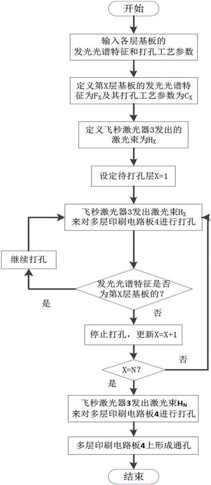
[0043] The laser drilling method of the multilayer printed circuit board of the present embodiment, as figure 1 As shown, including the process of punching holes into multilayer printed circuit boards:

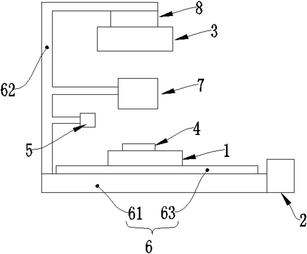
[0044] Step A1, place a multilayer printed circuit board 4 on the punching table 1, and the position to be punched of the multilayer printed circuit board 4 is aligned with the femtosecond / picosecond laser 3, and the multilayer printed circuit board 4 There are N layers of substrates with different materials from top to bottom along the thickness direction, N=2, 3, 4, ..., k, k≥2;

[0045] The femtosecond / picosecond laser 3 can switchably output laser beams of N different wavelengths to be used for etching substrates with N layers of different materials correspondingly;

[0046] Step A2, input the luminescence spectrum characteristics and punching process parameters of each layer substrate in the multilayer printed circuit board 4 in the industrial computer 2, and define the ...

Embodiment 2

[0076] A through hole with a diameter of 60 μm was drilled in the multilayer printed circuit board 4 by using the laser drilling method for the multilayer printed circuit board described in Embodiment 1. Such as Figure 4 As shown, the number of layers of the multilayer printed circuit board 4 in this embodiment is 4 layers, and the total thickness is 1.8mm. The material of the first layer substrate 42 and the third layer substrate 43 is red copper, and the second layer substrate 44 and the fourth layer substrate The material of the layer substrate 45 is FR-4 epoxy resin; the wavelength of the femtosecond / picosecond laser 3 is 800nm, the pulse width is 50fs, the highest laser beam repetition frequency is 1KHz, and the maximum laser beam pulse energy is 3mJ.

[0077] Specific steps are as follows:

[0078] Step 1, obtaining the luminescence spectrum characteristics of the conductive material copper used in the multilayer printed circuit board 4 and the insulating material FR-4...

Embodiment 3

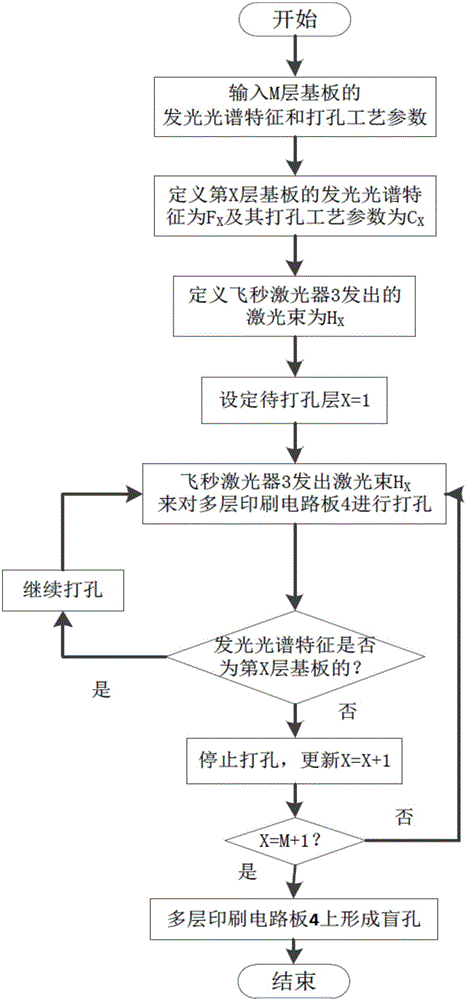
[0085] A blind hole with a diameter of 80 μm to the third layer substrate 43 is drilled on the multilayer printed circuit board 4 by using the laser drilling method for the multilayer printed circuit board described in Embodiment 1. In this embodiment, the number of layers of the multilayer printed circuit board 4 is 4 layers, and the total thickness is 1.8 mm. The materials of the first layer substrate 42 and the third layer substrate 43 are red copper, and the second layer substrate 44 and the fourth layer substrate 45 The material is FR-4 epoxy resin; the femtosecond / picosecond laser 3 has a wavelength of 800nm, a pulse width of 50fs, a maximum laser beam repetition frequency of 1KHz, and a maximum laser beam pulse energy of 3mJ.

[0086] Specific steps are as follows:

[0087]Step 1, obtaining the luminescence spectrum characteristics of the conductive material copper used in the multilayer printed circuit board 4 and the insulating material FR-4 epoxy resin under the acti...


PUM

PropertyMeasurementUnit
thicknessaaaaaaaaaa

Abstract

The invention discloses a laser punching method of a multilayer printed circuit board and a system using the same. The method comprises a process of punching a through hole in the multi-layer printed circuit board: (A1) the multilayer printed circuit board is placed on a punching worktable, a position to be punched of the multilayer printed circuit board is aligned to a femtosecond / picosecond laser, and the multi-layer printed circuit board is provided with N layers of substrates with different materials from top to bottom in the thickness direction; and the femtosecond / picosecond laser can output N laser beams with different wave lengths in a switching manner for correspondingly etching the N layers of substrates with different materials. The laser punching method of the multilayer printed circuit board comprises the process of punching the through hole in the multilayer printed circuit board and a process of punching a blind hole in the multilayer printed circuit board, realizes intelligent punching of the multilayer printed circuit board, intelligently identifies the punching layer number, automatically, quickly and accurately switches the femtosecond laser punching process parameters, is smooth in cross section of the machined through hole, and improves the punching quality and precision.

Description

technical field [0001] The invention relates to the field of printed circuit board processing and manufacturing, in particular to a laser drilling method for a multilayer printed circuit board and a system using the same. Background technique [0002] With the rapid development of electronic technology, multilayer printed circuit boards have been widely used in large-scale integrated circuits. The multilayer printed circuit board is formed by alternately pressing multiple layers of conductive substrates and multiple layers of insulating substrates, that is, a layer of insulating substrates is arranged between two adjacent layers of conductive substrates, and each layer of conductive substrates is arranged with different circuits and separated by insulating substrates; and A plurality of through holes and blind holes are provided on the multilayer printed circuit board for electrical connection between conductive substrates, and these through holes and blind holes are all mic...

Claims


Application Information

Patent Timeline
Patent Type & Authority Applications(China)
IPC IPC(8): B23K26/382B23K26/0622
CPCB23K26/0624B23K26/382B23K2101/42
Inventor 陈新刘强
Owner GUANGDONG UNIV OF TECH
Why Eureka
Try Eureka