A kind of superconductor-insulator-metal heterogeneous two-dimensional crystalline thin film material and preparation method thereof

A technology of thin film materials and insulators, which is applied in the field of superconductor-insulator-metal heterogeneous two-dimensional crystalline thin film materials and its preparation, can solve the problems of heterogeneous structure thin films with many defects, performance degradation, and easy contamination of the interface, and achieve a wide range of applications. Application potential, quality improvement, effect of less defects

Active Publication Date: 2019-02-05
INST OF PHYSICS - CHINESE ACAD OF SCI
View PDF5 Cites 0 Cited by
  • Summary
  • Abstract
  • Description
  • Claims
  • Application Information

AI Technical Summary

Problems solved by technology

At present, the commonly used method for preparing the heterostructure of two-dimensional materials is the method of exfoliation transfer stacking, but this method increases the complexity of the preparation process, and the obtained heterostructure film has many defects, and the interface is easily contaminated, resulting in its performance. reduce

Method used


Image

  • A kind of superconductor-insulator-metal heterogeneous two-dimensional crystalline thin film material and preparation method thereof
  • A kind of superconductor-insulator-metal heterogeneous two-dimensional crystalline thin film material and preparation method thereof
  • A kind of superconductor-insulator-metal heterogeneous two-dimensional crystalline thin film material and preparation method thereof

Examples


Embodiment 1

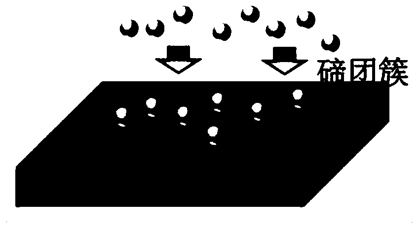
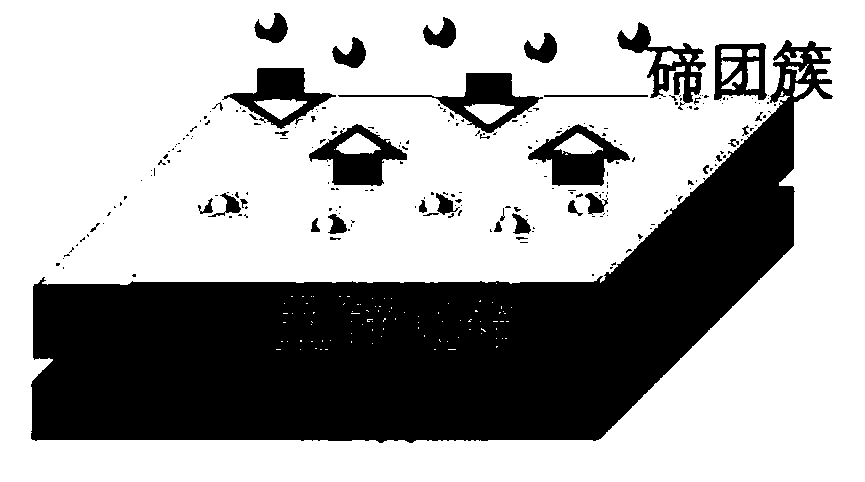
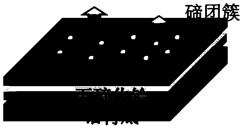
[0039]The hafnium single crystal was sputtered with argon ions for nearly 5 hours in a vacuum chamber, and then a clean and flat (0001) crystal plane was obtained by heating the metal hafnium substrate and maintaining it at a high temperature of 900 °C for 8 minutes. In a vacuum environment, an appropriate amount of high-purity tellurium was passed through a quartz crucible evaporation source, and metal tellurium was uniformly deposited on the surface of a hafnium substrate (0001) that was clean and flat and kept at room temperature. like figure 1 The tellurium particles shown are randomly distributed on the surface of the substrate, such as Figure 5 As shown in the scanning tunneling microscope image of , the samples deposited with tellurium particles were annealed at 500 °C for 15 minutes, so that the tellurium atoms covering the surface of the hafnium substrate (0001) interacted with the hafnium atoms of the substrate to form a hafnium pentatelluride film material ,like ...

Embodiment 2

[0041] The hafnium single crystal was sputtered with argon ions for nearly 3 hours in a vacuum chamber, and then a clean and flat (0001) crystal plane was obtained by heating the metal hafnium substrate and maintaining it at a high temperature of 900 °C for 5 minutes. In a vacuum environment, an appropriate amount of high-purity tellurium was passed through a quartz crucible evaporation source, and metal tellurium was uniformly deposited on the surface of a hafnium substrate (0001) that was clean and flat and kept at room temperature. The tellurium particles are randomly distributed on the surface of the substrate. The samples deposited with the tellurium particles were annealed at 450 °C for 10 minutes, so that the tellurium atoms covering the surface of the hafnium substrate (0001) interacted with the hafnium atoms of the substrate to form hafnium pentatelluride. The film material is a periodic superstructure that can be characterized by scanning tunneling microscopy, which a...

Embodiment 3

[0043] The hafnium single crystal was sputtered with argon ions for nearly 6 hours in a vacuum chamber, and then a clean and flat (0001) crystal plane was obtained by heating the metal hafnium substrate and maintaining it at a high temperature of 900 °C for 10 minutes. In a vacuum environment, an appropriate amount of high-purity tellurium was passed through a quartz crucible evaporation source, and metal tellurium was uniformly deposited on the surface of a hafnium substrate (0001) that was clean and flat and kept at room temperature. The tellurium particles are randomly distributed on the surface of the substrate. The samples deposited with the tellurium particles were annealed at 500 °C for 10 minutes, so that the tellurium atoms covering the surface of the hafnium substrate (0001) interacted with the hafnium atoms of the substrate to form hafnium pentatelluride. The film material is a periodic superstructure that can be characterized by scanning tunneling microscopy, which ...


PUM


Abstract

The invention discloses a superconductor-insulator-metal heterogeneous film material which is of a laminated structure. The superconductor-insulator-metal heterogeneous film material comprises a metal hafnium base layer, a hafnium pentatelluride film structure layer and a hafnium tritelluride film structure layer, and the laminated structure is expanded in a two-dimensional plane. A preparing method includes the steps that a proper amount of high-purity hafnium is evaporated and deposited to the surface of the transition metal hafnium base layer in a vacuum environment; annealing treatment is conducted so that deposited tellurium atoms and metal hafnium atoms on the base interact with each other to form a hafnium pentatelluride two-dimensional orderly crystalline film-shaped structure; and annealing treatment is further conducted, the surface of the formed hafnium pentatelluride two-dimensional orderly crystalline film-shaped structure is subjected to the structure change again to form hafnium tritelluride, finally, the hafnium tritelluride-hafnium pentatelluride-metal hafnium two-dimensional laminated structure is formed, and the superconductor-insulator-metal heterogeneous film material is obtained. The preparing technology is relatively simple, defects of the obtained heterogeneous-structure film are few, an interface is not likely to be polluted, and the quality of the heterogeneous-structure film is improved.

Description

technical field [0001] The invention belongs to the technical field of nanomaterials, and in particular relates to a superconductor-insulator-metal heterogeneous two-dimensional crystalline thin film material and a preparation method thereof. Background technique [0002] Graphene, as a classic representative of two-dimensional crystalline materials, has become a worldwide research hotspot in just ten years since it was stripped from its parent graphite in 2004 due to its unique electronic and physical properties. The exploration and research boom of two-dimensional crystalline materials. Stacking two-dimensional crystalline materials with different physical properties is very likely to produce some new material structures and physical properties. For example, in the graphene-boron nitride heterostack structure, new physical properties have been observed (Hofsch Tate Butterfly - a wonderful fractal pattern describing the movement of electrons in a magnetic field); this grap...

Claims


Application Information

Patent Timeline
Patent Type & Authority Patents(China)
IPC IPC(8): C23C14/06C23C14/24C23C14/58C23C14/02
Inventor 王业亮
Owner INST OF PHYSICS - CHINESE ACAD OF SCI
Why Eureka
Try Eureka