Method for increasing OPC (Optical Proximity Correction) processing accuracy

A precision and similarity technology, applied in the field of enhanced OPC processing precision for high MEEF graphics, can solve the problem of low graphics precision, achieve the effects of reducing running time, improving processing efficiency, reducing complexity and running time

Active Publication Date: 2017-05-24
SHANGHAI HUALI MICROELECTRONICS CORP
View PDF6 Cites 5 Cited by
  • Summary
  • Abstract
  • Description
  • Claims
  • Application Information

AI Technical Summary

Problems solved by technology

[0007] The purpose of the present invention is to overcome the above-mentioned defects existing in the prior art, and provide a method for enhancing the precision of OPC processing, which is used to impr

Method used


Image

  • Method for increasing OPC (Optical Proximity Correction) processing accuracy
  • Method for increasing OPC (Optical Proximity Correction) processing accuracy
  • Method for increasing OPC (Optical Proximity Correction) processing accuracy

Examples


Embodiment Construction

[0033] The present invention provides a method and system for improving OPC processing layout inconsistency, so as to improve the problem of different random correction results in different places of repeated graphic areas, and at the same time greatly reduce the running time of the system. The following example of the present invention provides an improved method and system for OPC processing layout, which can not only overcome the randomness of traditional design and data redundancy, improve the processing efficiency of layout, but also reduce the complexity and running time of OPC processing. The present invention will be further described below in conjunction with the accompanying drawings.

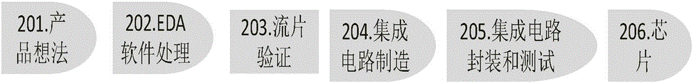
[0034] figure 2 The stages of integrated circuits from design to fabrication are shown. The process of chip generation generally includes the following steps:

[0035] Step 201. Product idea;

[0036] Step 202.EDA software processing;

[0037] Step 203. Tape-out verification;

...


PUM


Abstract

The invention discloses a method for increasing OPC (Optical Proximity Correction) processing accuracy. Hotspot analysis and MEEF (Mask Error Enhancement Factor) value judgment are performed on publishing data by using information for building a process hotspot library, enhanced OPC graph correction and check are carried out on a high-MEEF graph of which the MEEF value is higher than a set value, and the process hotspot library is continually upgraded on the basis, so that the problem of different results of random correction at different places in overlapped graph areas during the conventional OPC correction is solved, the OPC processing accuracy of the high-MEEF graph is increased, and the consistence of OPC correction results is kept; the method can be compatible with an existing processing method; meanwhile the running time of a system can be shortened greatly, the randomness and data redundancy in the conventional design are overcome, the layout processing efficiency is increased, and the complexity and running time of OPC processing can be lowered and shortened.

Description

technical field [0001] The invention relates to the technical field of integrated circuit manufacturing, and more specifically relates to a method for enhancing OPC processing precision for high MEEF graphics. Background technique [0002] At present, large-scale integrated circuits are generally manufactured using photolithography systems. The lithography system is mainly divided into four systems: illumination system, mask, projection system and silicon wafer. figure 1 Demonstrates the principles of optical transport in lithography systems. The light emitted from the light source 202 of the illumination system is incident on the mask 206 after being focused by the condenser lens 204, and the opening part of the mask is light-transmitting; after passing through the mask, the light is incident on the wafer coated with photoresist through the hole 208 and the lens 210 of the projection system (silicon wafer) 212, so that the mask pattern is replicated on the wafer. [0003...

Claims


Application Information

Patent Timeline
IPC IPC(8): G03F1/36G03F7/20G06F17/50
CPCG03F1/36G03F7/70441G06F30/39
Inventor 孟鸿林魏芳朱骏
Owner SHANGHAI HUALI MICROELECTRONICS CORP
Why Eureka
Try Eureka