Circuit-level modeling method and model circuit which are used for GGNMOS

A modeling method and circuit technology, applied in CAD circuit design, electrical digital data processing, special data processing applications, etc., can solve problems such as low efficiency, time-consuming physical-level modeling, and increased design costs, achieving high efficiency, Simple structure and low design cost

Active Publication Date: 2017-05-24
SHENZHEN STATE MICROELECTRONICS CO LTD
View PDF5 Cites 7 Cited by
  • Summary
  • Abstract
  • Description
  • Claims
  • Application Information

AI Technical Summary

Problems solved by technology

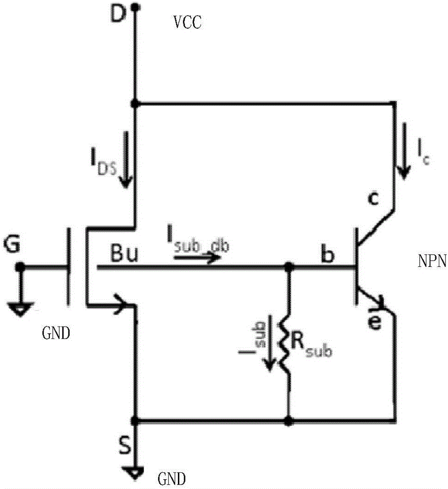
The commonly used SPICE simulation does not provide these complex calculations. The existing common method is to first conduct physical-level modeling and simulation of GGNMOS, extract relevant parameters, and then perform circuit-level simulation.
There are many ways to extract parameters by physical modeling, which can be realized by TCAD, MATLAB, Verilog-A and other software, but physical-level modeling is time-consuming, inefficient, and increases design costs

Method used


Image

  • Circuit-level modeling method and model circuit which are used for GGNMOS
  • Circuit-level modeling method and model circuit which are used for GGNMOS
  • Circuit-level modeling method and model circuit which are used for GGNMOS

Examples


Embodiment

[0049] Embodiment: Taking SMIC65nm process standard IO as an example, how to realize the equivalent circuit model of GGNMOS in the present invention is illustrated.

[0050] Figure 4 It is the GGNMOS schematic diagram of the standard IO provided by the SMIC process, such as Figure 4 As shown, the peripheral ring P+sub-ring represents the P-type implanted substrate ring, which is divided into three regions A, B, and C, including 18 GGNMOS devices, numbered Q0-Q17 respectively, and the GNNMOSs in each region are connected in parallel. relation.

[0051] Figure 5 yes Figure 4 In the connection relationship between the ports of each device of Q0-Q17, the gates, sources and substrates of the GGNMOS devices Q0-Q17 are all connected to the power ground, and the drains are connected to the power potential.

[0052] Image 6 yes figure 1 The enlarged view of the area A in the middle, SAB represents the silicide barrier layer of the drain region, ESD1 represents the ESD inject...


PUM


Abstract

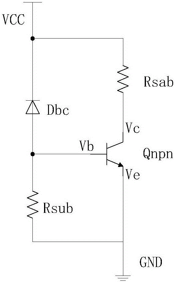
The invention discloses a circuit-level modeling method and a model circuit which are used for a GGNMOS. The model circuit comprises a triode, a first resistor, a second resistor and a diode. One end of the first resistor is in connection with a power ground, the other end of the first resistor is connected with the positive pole of the diode, the negative pole of the diode is connected with a power supply, the base of the triode is connected with a connection node between the diode and the first resistor, the emitter of the triode is connected with the power ground, and the collector of the triode is connected with the power supply through the second resistor. According to the circuit-level modeling method used for the GGNMOS, modeling is conducted on the GGNMOS, the clamping ability that the GGNMOS impacts on an ESD can be obtained by simulation within a short time by means of the model circuit, the structure is simple, the method is simple to implement, compared with an existing method that physical modeling is conducted by adopting a parameter extraction mode, the efficiency is higher, and the design cost is low.

Description

technical field [0001] The invention relates to the field of integrated circuit design, in particular to a circuit-level modeling method and model circuit for GGNMOS. Background technique [0002] ESD: Electro-Static discharge, electrostatic discharge. [0003] GGNMOS: GATE GROUNDED NMOS tube, gate grounded NMOS tube. [0004] TLP: Transmission Line Puls, transmission line pulse test, is a chip reliability test method, by measuring the current value of the ESD protection unit when it breaks down for the second time, the maximum anti-ESD ability of the protection ESD unit can be estimated. [0005] With the integration level of integrated circuits getting higher and higher, and the feature size getting smaller and smaller, ESD protection design is facing more and more severe challenges. The GGNMOS structure is currently a more common ESD structure. Since the GGNMOS is a breakdown discharge, it cannot be directly simulated at the circuit level. [0006] According to the typ...

Claims


Application Information

Patent Timeline
Patent Type & Authority Applications(China)
IPC IPC(8): G06F17/50
CPCG06F30/36G06F30/367
Inventor 贾柱良何凯杨君
Owner SHENZHEN STATE MICROELECTRONICS CO LTD
Why Eureka
Try Eureka